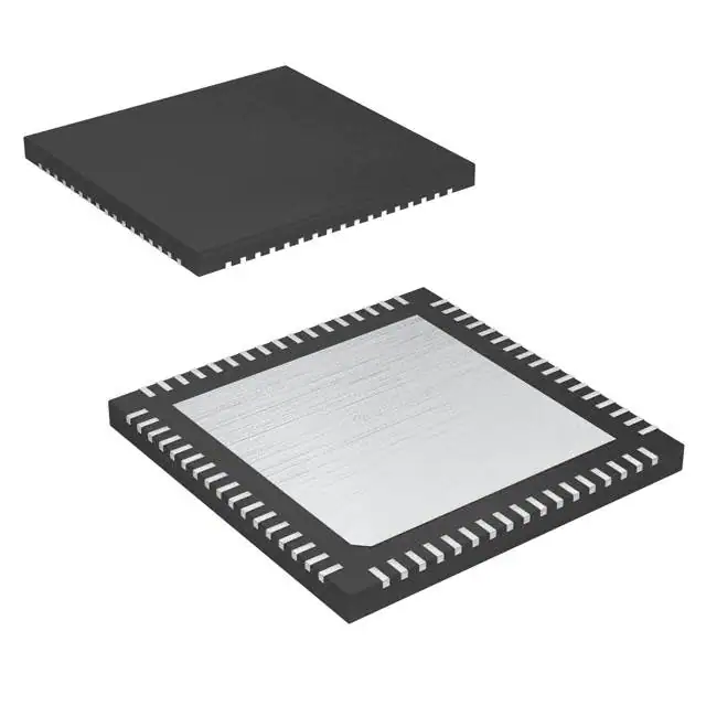
ProASIC3, the third-generation family of Microsemi flash FPGAs, offers performance, density, and features beyond those of the ProASICPLUS® family. Nonvolatile flash technology gives ProASIC3 devices the advantage of being a secure, low power, single-chip solution that is Instant On. ProASIC3 is reprogrammable and offers time-to-market benefits at an ASIC-level unit cost. These features enable designers to create high-density systems using existing ASIC or FPGA design flows and tools.
ProASIC3 devices offer 1 kbit of on-chip, reprogrammable, nonvolatile FlashROM storage as well as clock conditioning circuitry based on an integrated phase-locked loop (PLL). The A3P015-QNG68I and A3P030 devices have no PLL or RAM support.
ProASIC3 devices have up to 1 million system gates, supported with up to 144 kbits of true dual-port SRAM and up to 300 user I/Os. ProASIC3 devices support the ARM Cortex-M1 processor. The ARM-enabled devices have Microsemi ordering numbers that begin with M1A3P (Cortex-M1) and do not support AES decryption.
Feature
• 15 K to 1 M System Gates
• Up to 144 Kbits of True Dual-Port SRAM
• Up to 300 User I/Os
Reprogrammable Flash Technology
• 130-nm, 7-Layer Metal (6 Copper), Flash-Based CMOS Process
• Instant On Level 0 Support
• Single-Chip Solution
• Retains Programmed Design when Powered Off
High Performance
• 350 MHz System Performance
• 3.3 V, 66 MHz 64-Bit PCI†
In-System Programming (ISP) and Security
• ISP Using On-Chip 128-Bit Advanced Encryption Standard (AES) Decryption (except ARM®-enabled ProASIC®3 devices) via JTAG (IEEE 1532–compliant)†
• FlashLock® to Secure FPGA Contents
Low Power
• Core Voltage for Low Power
• Support for 1.5 V-Only Systems
• Low-Impedance Flash Switches
High-Performance Routing Hierarchy
• Segmented, Hierarchical Routing and Clock Structure


