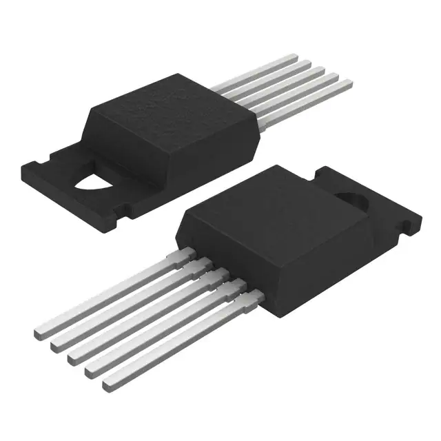
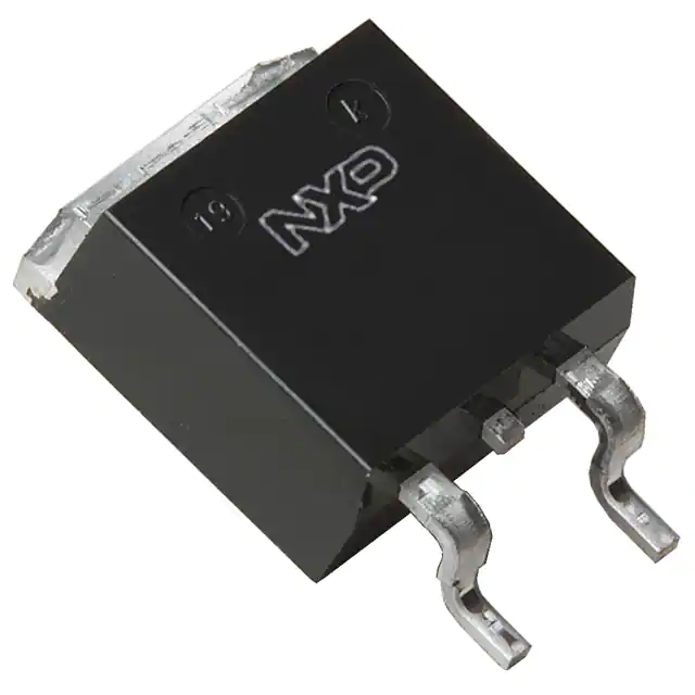
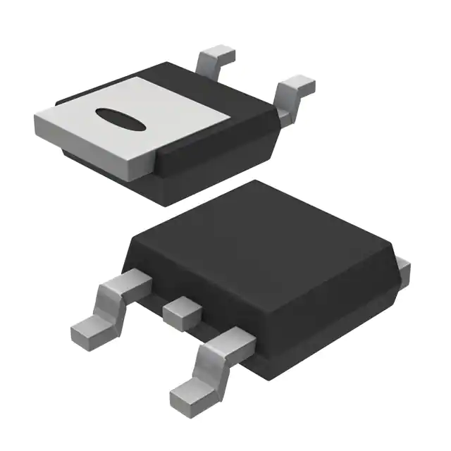
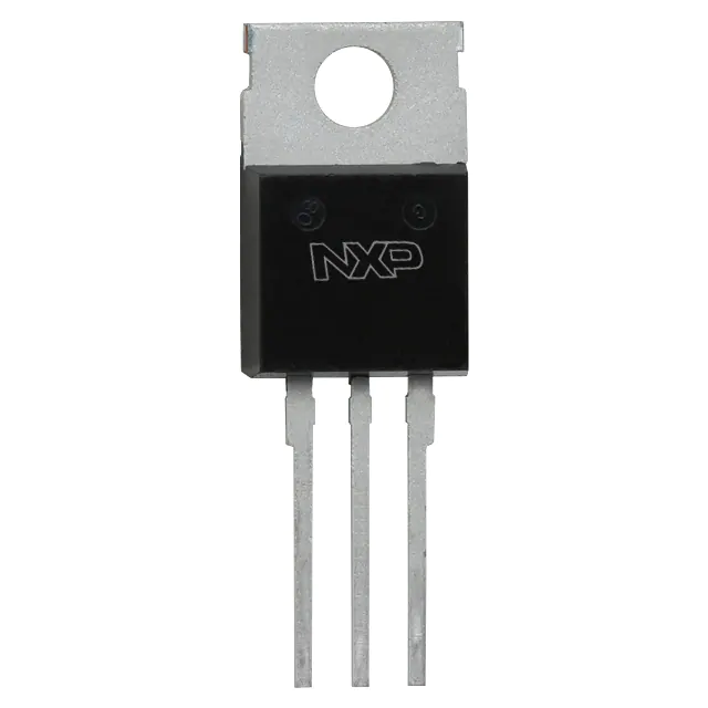
9icnet provides you with BUK7Y13-40B,115 designed and produced by NXP USA Inc., which is sold in 9icnet on the spot, and can be purchased through channels such as the original factory and agents. BUK7Y13-40B,115 price reference $0.28000. NXP USA Inc. BUK7Y13-40B,115 Package/Specification: MOSFET N-CH 40V 58A LFPAK. You can download BUK7Y13-40B,115 english data, pin diagram, Datasheet data sheet function manual, the data contains detailed pin diagrams of diode rectifiers, application circuit diagrams of functions, voltages, usage methods and tutorials.
Prices and stocks marked on 9icnet are for reference only. If you don't find what you are looking for, you can contact us by email or online message, such as BUK7Y13-40B,115 price, stock quantity, data sheet and manufacturer. We look forward to your contact and provide you with quality service.
BUK7Y12-40EX with pin details, that includes Reel Packaging, they are designed to operate with a BUK7Y12-40E115 Part Aliases, Mounting Style is shown on datasheet note for use in a SMD/SMT, that offers Package Case features such as LFPAK-4, Technology is designed to work in Si, as well as the 1 Channel Number of Channels, the device can also be used as Single Configuration. In addition, the Transistor Type is 1 N-Channel, the device is offered in 65 W Pd Power Dissipation, it has an Maximum Operating Temperature range of + 175 C, it has an Minimum Operating Temperature range of - 55 C, and the Fall Time is 6 ns, and Rise Time is 7 ns, and the Vgs Gate Source Voltage is 20 V, and Id Continuous Drain Current is 52 A, and the Vds Drain Source Breakdown Voltage is 40 V, and Vgs th Gate Source Threshold Voltage is 3 V, and the Rds On Drain Source Resistance is 9.3 mOhms, and Transistor Polarity is N-Channel, and the Typical Turn Off Delay Time is 10 ns, and Typical Turn On Delay Time is 6 ns, and the Qg Gate Charge is 15 nC, and Channel Mode is Enhancement.
BUK7Y12-100EX with user guide, that includes 3 V Vgs th Gate Source Threshold Voltage, they are designed to operate with a 20 V Vgs Gate Source Voltage, Vds Drain Source Breakdown Voltage is shown on datasheet note for use in a 100 V, that offers Typical Turn On Delay Time features such as 12 ns, Typical Turn Off Delay Time is designed to work in 66 ns, as well as the 1 N-Channel Transistor Type, the device can also be used as N-Channel Transistor Polarity. In addition, the Technology is Si, the device is offered in 18 ns Rise Time, the device has a 8.1 mOhms of Rds On Drain Source Resistance, and Qg Gate Charge is 68 nC, and the Pd Power Dissipation is 238 W, and Packaging is Reel, and the Package Case is LFPAK-4, and Number of Channels is 1 Channel, and the Mounting Style is SMD/SMT, it has an Minimum Operating Temperature range of - 55 C, it has an Maximum Operating Temperature range of + 175 C, and Id Continuous Drain Current is 85 A, and the Fall Time is 66 ns, and Configuration is Triple Common Source.
The BUK7Y12-55B,115 is MOSFET N-CH 55V 61.8A LFPAK, that includes 61.8A (Tc) Current Continuous Drain Id 25°C, they are designed to operate with a 55V Drain to Source Voltage Vdss, FET Feature is shown on datasheet note for use in a Standard, that offers FET Type features such as MOSFET N-Channel, Metal Oxide, Gate Charge Qg Vgs is designed to work in 35.2nC @ 10V, as well as the 2067pF @ 25V Input Capacitance Ciss Vds, the device can also be used as Surface Mount Mounting Type, it has an Operating Temperature range of -55°C ~ 175°C (TJ), the device is offered in SC-100, SOT-669, 4-LFPAK Package Case, the device has a Digi-ReelR Alternate Packaging of Packaging, and Power Max is 105W, and the Rds On Max Id Vgs is 12 mOhm @ 20A, 10V, and Series is Automotive, AEC-Q101, TrenchMOS?, and the Supplier Device Package is LFPAK, Power-SO8, and Vgs th Max Id is 4V @ 1mA.
BUK7Y12-80EX with EDA / CAD Models, that includes Si Technology, they are designed to operate with a Reel Packaging.


