All trademarks are the property of their respective owners.
DescriptionThe TPS65150-Q1 is an integrated power-supply for automotive LCD applications. The deviceintegrates a boost converter for the source voltage and two regulated adjustable charge pumpdrivers for the gate voltages. For reduced external cost, improved picture quality and reducedimage sticking, the device includes a VCOM buffer and a gate-voltage shaping function.
The device is designed to operate from a supply voltage of 1.8 V to 6 V making it idealfor automotive LCD applications using a fixed 3.3 V or 5 V input-voltage rail.
Adjustable power-on sequencing for VGL and VGH allow the device to be optimized for avariety of displays.
For protection from system malfunction, the TPS65150-Q1 integrates an adjustable shutdownlatch feature. The device monitors the outputs (V(VS),V(VGL), V(VGH)); and, as soon as one of the outputsfalls below its power-good threshold for longer than the adjustable fault delay time, the deviceenters shutdown.
Feature
- AEC-Q100 Qualified:
- Device Temperature Grade 1: –40°C to 125°C JunctionTemperature
- Device HBM ESD Classification According to AEC -Q100-002
- Device CDM ESD Classification According to AEC -Q100-011
- Input Voltage Range: 1.8 V to 6 V
- V(VS) Boost Converter
- Up to 15 V Output Voltage
- < 1% Output Voltage Accuracy
- 2-ASwitch Current Limit
- V(VGH)Positive Regulated Charge Pump Driver
- Up to 30 V Output Voltage
- Gate Voltage Shaping
- V(VGL)Negative Regulated Charge Pump Driver
- Down to –15 V Output Voltage
- Integrated VCOM Buffer
- Adjustable Power On Sequencing
- Gate Drive Signal for External Isolation MOSFET forV(VS)
- Protection
- Out-of-Regulation Protection
- Over-voltage Protection
- AdjustableFault Detection Timing
- Thermal Shutdown
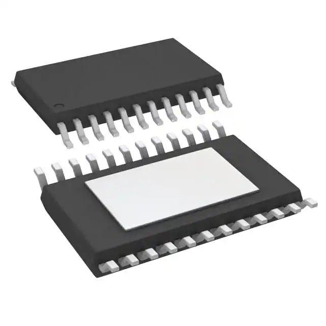
- 24-Pin TSSOP Package with Exposed Thermal Pad
All trademarks are the property of their respective owners.
DescriptionThe TPS65150-Q1 is an integrated power-supply for automotive LCD applications. The deviceintegrates a boost converter for the source voltage and two regulated adjustable charge pumpdrivers for the gate voltages. For reduced external cost, improved picture quality and reducedimage sticking, the device includes a VCOM buffer and a gate-voltage shaping function.
The device is designed to operate from a supply voltage of 1.8 V to 6 V making it idealfor automotive LCD applications using a fixed 3.3 V or 5 V input-voltage rail.
Adjustable power-on sequencing for VGL and VGH allow the device to be optimized for avariety of displays.
For protection from system malfunction, the TPS65150-Q1 integrates an adjustable shutdownlatch feature. The device monitors the outputs (V(VS),V(VGL), V(VGH)); and, as soon as one of the outputsfalls below its power-good threshold for longer than the adjustable fault delay time, the deviceenters shutdown.


