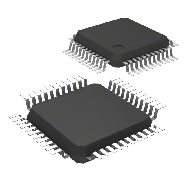
The Lattice ispPAC-POWR1208 incorporates both insystem programmable logic and in-system programmable analog circuits to perform special functions for power supply sequencing and monitoring. The ispPACPOWR1208 device has the capability to be configured through software to control up to eight outputs for power supply sequencing and 12 comparators monitoring supply voltage limits, along with four digital inputs for interfacing to other control circuits or digital logic. Once configured, the design is downloaded into the device through a standard JTAG interface. The circuit configuration and routing are stored in non-volatile E2 CMOS. PAC-Designer,® an easy-to-use Windows-compatible software package gives users the ability to design the logic and sequences that control the power supplies or FET driver circuits. The user has control over timing functions, programmable logic functions and comparator threshold values as well as I/O configurations.
The ispPAC-POWR1208 device is specifically designed as a fully-programmable power supply sequencing controller and monitor for managing up to eight separate power supplies, as well as monitoring up to 12 analog inputs or supplies. The ispPAC-POWR1208 device contains an internal PLD that is programmable by the user to implement digital logic functions and control state machines. The internal PLD connects to four programmable timers, special purpose I/O and the programmable monitoring circuit blocks. The internal PLD and timers can be clocked by either an internal programmable clock oscillator or an external clock source.
The voltage monitors are arranged as 12 independent comparators each with 192 programmable trip point settings. Monitoring levels are set around the following standard voltages: 1.2V, 1.5V, 1.8V, 2.5V, 3.3V or 5.0V.
All 12 voltages can be monitored simultaneously (i.e., continuous-time operation). Other non-standard voltage levels can be accounted for using various scale factors.
For added robustness, the comparators feature a variable hysteresis that scales with the voltage they monitor. Generally, a larger hysteresis is better. However, as power supply voltages get smaller, that hysteresis increasingly affects trip-point accuracy. Therefore, the hysteresis is +/-16mV for 5V supplies and scales down to +/-3mV for 1.2V supplies, or about 0.3% of the trip point.
The programmable logic functions consist of a block of 36 inputs with 81 product terms and 16 macrocells. The architecture supports the sharing of product terms to enhance the overall usability. Output pins are configurable in two different modes. There are eight outputs for controlling eight different power supplies. OUT5-OUT8 are open-drain outputs for interfacing to other circuits. The HVOUT1-HVOUT4 pins can be programmed individually as open-drain outputs or as high voltage FET gate drivers. As high voltage FET gate driver outputs, they can be used to drive an external N-Channel MOSFET as a switch to control the voltage rampup of the target board. The four HVOUT drivers have programmable current and voltage levels. Of the eight outputs, four can be configured in the FET gate driver mode or open-drain digital mode.
Feature
■ Monitor and Control Multiple Power Supplies
• Simultaneously monitors up to 12 power supplies
• Sequence controller for power-up conditions
• Provides eight output control signals
• Programmable digital and analog circuitry
■ Embedded PLD for Sequence Control
• Implements state machine and input conditional events
• In-System Programmable (ISP™) through JTAG and on-chip E2 CMOS®
■ Embedded Programmable Timers
• 4 Programmable 8-bit timers (32µs to 524ms)
• Programmable time delay between multiple power supply ramp-up and wait statements
■ Analog Comparators for Monitoring
• 12 analog comparators for monitoring
• 192 precise programmable threshold levels spanning 1.03V to 5.72V
• Each comparator can be independently configured around standard logic supply voltages of 1.2V, 1.5V, 1.8V, 2.5V, 3.3V, 5V
• Other user-defined voltages possible
• Eight direct comparator outputs
■ Embedded Oscillator
• Built-in clock generator, 250kHz
• Programmable clock frequency
• Programmable timer pre-scaler
• External clock support
■ Programmable Output Configurations
• Four digital outputs for logic and power supply control
• Four fully programmable gate driver outputs for FET control, or programmable as four additional digital outputs
• Expandable with ispMACH™ 4000 CPLD
■ 2.25V to 5.5V Supply Range
• In-system programmable at 3.0V to 5.5V
• Industrial temperature range: -40°C to +85°C
• Automotive temperature range: -40°C to +125°C
• 44-pin TQFP package
• Lead-free package option
(Picture: Pinout)


