
This device, together with a PIN diode and a TIA preamplifier, can implement a highly integrated, low cost, and low power fiber optic receiver.
The ADN2817/ADN2818 have many optional features available through an I2C interface. For example, the user can read back the data rate onto which the ADN2817ACPZ-RL7 or ADN2818 is locked, or the user can set the device to lock only to one particular data rate if provisioning of data rates is required. A BERMON circuit provides an estimate of the received bit error rate (BER) without interruption of the data. Alternatively, the user can adjust the data sampling phase to optimize the received BER.
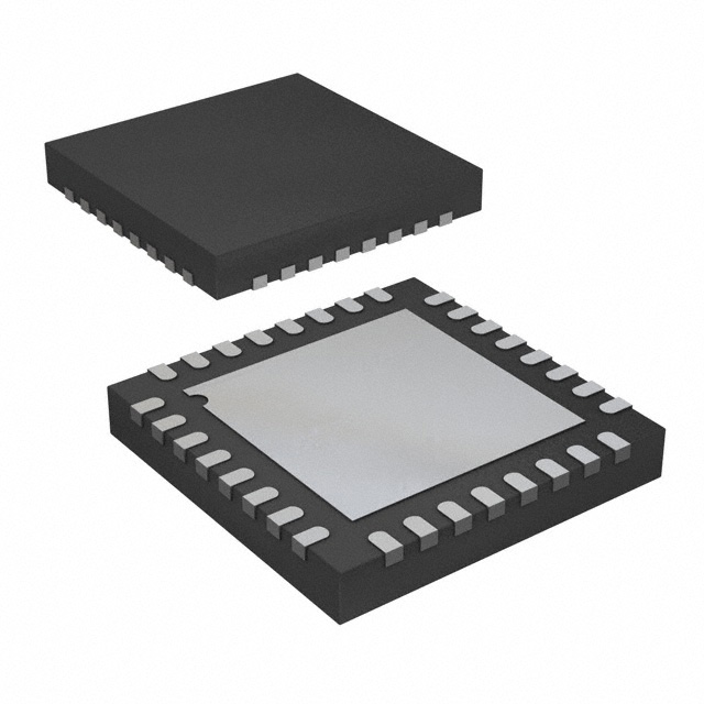
The ADN2817/ADN2818 are available in a compact 5 mm × 5 mm, 32-lead, lead frame chip scale package.
Feature
- Serial data input: 10 Mbps to 2.7 Gbps
- Exceeds ITU-T jitter specifications
- Integrated limiting amplifier
- 5 mV p-p sensitivity ( only)
- Adjustable slice level: ±100 mV ( only)
- Proprietary dual-loop clock recovery architecture
- Programmable LOS detect ( only)
- Integrated PRBS generator and detector
- No reference clock required
- Loss of lock indicator
- Supports double data rate
- BERMON or sample phase adjust options
- Rate selectivity without the use of a reference clock
- I2C interface to access optional features
- Single-supply operation: 3.3 V
- Low power
- 650 mW ()
- 600 mW ()
- 5 mm × 5 mm 32-lead LFCSP
Applications
- SONET OC-1, OC-3, OC-12, OC-48, and all associated FEC rates
- Fibre Channel, 2× Fibre Channel, GbE, HDTV, and others
- WDM transponders
- Regenerators/repeaters
- Test equipment
Data Sheet, Rev. A, 8/08
(Picture: Pinout)


