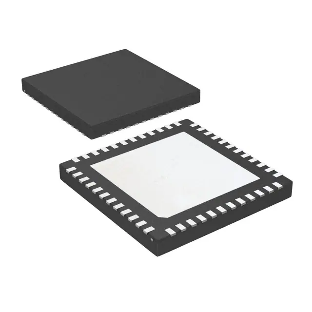
The LMK01801BISQ/NOPB is a very low noise solution for clocking systems that requiredistribution and frequency division of precision clocks.
The LMK01801BISQ/NOPB features extremely low residual noise, frequency division, digital andanalog delay adjustments, and fourteen (14) programmable differential outputs: LVPECL, LVDS andLVCMOS (2 outputs per differential output).
The LMK01801BISQ/NOPB features two independent inputs that can be driven differentially (LVDS,LVPECL) or in single-ended mode (LVCMOS, RF Sinewave). The first input drives output Bank Aconsisting of eight (8) outputs. The second input drives output Bank B consisting of six (6)outputs.
Feature
- Pin Control Mode or MICROWIRE (SPI)
- Input and Output Frequency Range 1 kHz to 3.1 GHz
- Separate Input for Clock Output Banks A & B.
- 14 Differential Clock Outputs in Two Banks (A & B)
- Output Bank A
- 8 Differential, Programmable Outputs (Up to 8 as LVCMOS)
- Divider Values of 1 to 8, Even and Odd.
- Output Bank B
- 6 Differential Outputs (or up to 12 as LVCMOS)
- Divides Values of 1 to 1045 or 1 to 8, Even and Odd
- Analog and Digital Delays
- Output Bank A
- 50% Duty Cycle on All Outputs for All Divides
- Separate Synchronization of Bank A and B.
- RMS Additive Jitter 50 fs at 800 MHz
- 50 fs RMS Additive Jitter (12 kHz to 20 MHz)
- Industrial Temperature Range: –40 to 85°C
- 3.15 V to 3.45 V Operation

