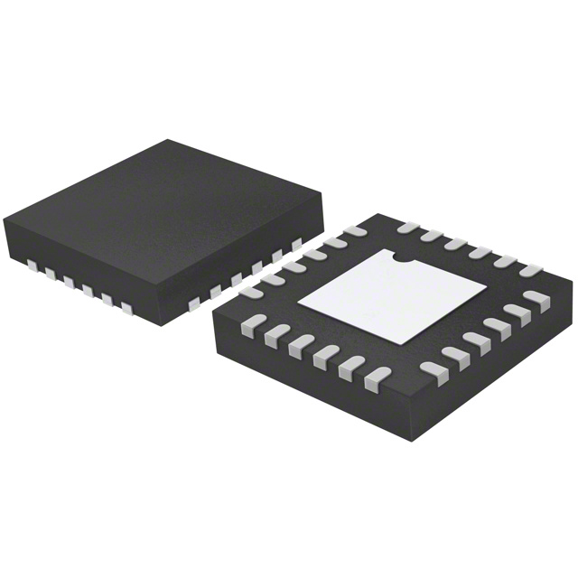
The AD9508BCPZ-REEL7 provides clock fanout capability in a design thatemphasizes low jitter to maximize system performance. Thisdevice benefits applications like clocking data converters withdemanding phase noise and low jitter requirements.
There are four independent differential clock outputs, each withvarious types of logic levels available. Available logic typesinclude LVDS (1.65 GHz), HSTL (1.65 GHz), and 1.8 V CMOS(250 MHz). In 1.8 V CMOS output mode, the differential outputbecomes two CMOS single-ended signals. The CMOS outputsare 1.8 V logic levels, regardless of the operating supply voltage.
Each output has a programmable divider that can be bypassedor be set to divide by any integer up to 1024. In addition, theAD9508BCPZ-REEL7 supports a coarse output phase adjustment betweenthe outputs.
The device can also be pin programmed for various fixedconfigurations at power-up without the need for SPI or I2C programming.
The AD9508BCPZ-REEL7 is available in a 24-lead LFCSP and operates froma either a single 2.5 V or 3.3 V supply. The temperature range is−40°C to +85°C.
Feature
- 1.65 GHz differential clock inputs/outputs
- 10-bit programmable dividers, 1 to 1024, all integers
- Up to 4 differential outputs or 8 CMOS outputs
- Pin strapping capability for hardwired programming at power-up
- <115 fs rms broadband random jitter
- Additive output jitter: 41 fs rms typical (12 kHz to 20 MHz)
- Excellent output-to-output isolation
- Automatic synchronization of all outputs
- Single 2.5 V/3.3 V power supply
- Internal LDO (low drop-out) voltage regulator for enhanced power supply immunity
- Phase offset select for output-to-output coarse delay adjust
- 3 programmable output logic levels, LVDS, HSTL, and CMOS
- Serial control port (SPI/I2C) or pin-programmable mode
- Space-saving 24-lead LFCSP
- Download (pdf)
- Extended temperature range: −55°C to +105°C
- Controlled manufacturing baseline
- One assembly/test site
- One fabrication site
- Enhanced product change notification
- Qualification data available on request
- V62/13626 DSCC Drawing Number
Applications
- Low jitter, low phase noise clock distribution
- Clocking high speed ADCs, DACs, DDSs, DDCs, DUCs, MxFEs
- High performance wireless transceivers
- High performance instrumentation
- Broadband infrastructure
(Picture: Pinout)


