The ADP7159ACPZ-02-R7 is an adjustable linear regulator that operates from 2.3 V to 5.5 V and provides up to 2 A of output current. Output voltages from 1.2 V to 3.3 V are possible depending on the model. Using an advanced proprietary architecture, the device provides high power supply rejection and ultralow noise, achieving excellentline and load transient response with only a 10 μF ceramicoutput capacitor.
The ADP7159ACPZ-02-R7 is available in four models that optimize powerdissipation and PSRR performance as a function of the inputand output voltage.
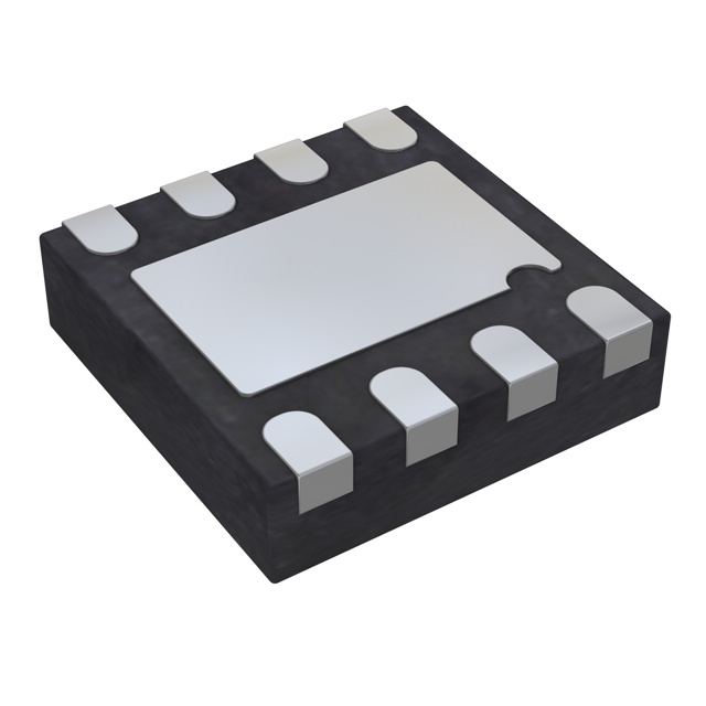
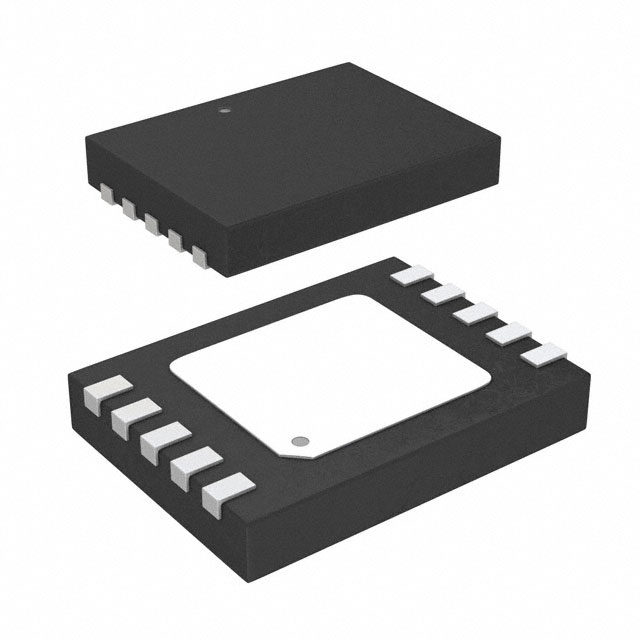
The typical output noise of the ADP7159ACPZ-02-R7 regulator is 0.9 μV rmsfrom 100 Hz to 100 kHz and 1.7 nV/√Hz for noise spectral densityfrom 10 kHz to 1 MHz. The ADP7159ACPZ-02-R7 is available in 10-lead,3 mm × 3 mm LFCSP and 8-lead SOIC packages, making it notonly a very compact solution, but also providing excellent thermal performance for applications requiring up to 2 A of outputcurrent in a small, low profile footprint.
Feature
- Input voltage range: 2.3 V to 5.5 V
- Adjustable output voltage range (VOUT): 1.2 V to 3.3 V
- Maximum load current: 2 A
- Low noise
- 0.9 μV rms total integrated noise from 100 Hz to 100 kHz
- 1.6 μV rms total integrated noise from 10 Hz to 100 kHz
- Noise spectral density: 1.7 nV/√Hz from 10 kHz to 1 MHz
- Power supply rejection ratio (PSRR)
- 68 dB from 1 kHz to 100 kHz
- 45 dB at 1 MHz
- Dropout voltage: 200 mV typical at IOUT = 2 A, VOUT = 3.3 V
- Initial accuracy: ±0.6% at ILOAD = 10 mA
- Accuracy over line, load, and temperature: ±1.5%
- See data sheet for additional features
Applications
- Regulation to noise sensitive applications: phase-lockedloops (PLLs), voltage controlled oscillators (VCOs), andPLLs with integrated VCOs
- Communications and infrastructure
- Backhaul and microwave links
(Picture: Pinout)


