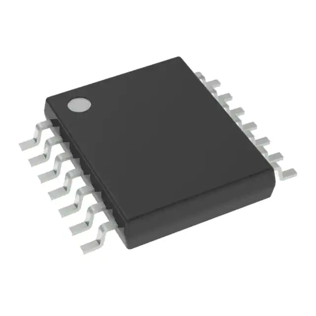
The TLC555CPW is a monolithic timing circuit fabricated using the TILinCMOS process. The timer is fully compatiblewith CMOS, TTL, and MOS logic and operates at frequencies up to 2 MHz. Because of its high inputimpedance, this device supports smaller timing capacitors than those supported by the NE555 orLM555. As a result, more accurate time delays and oscillations are possible. Power consumption islow across the full range of power-supply voltage.
Like the NE555, the TLC555CPW has a trigger level equal to approximately one-third of thesupply voltage and a threshold level equal to approximately two-thirds of the supply voltage. Theselevels can be altered by use of the control voltage terminal (CONT). When the trigger input (TRIG)falls below the trigger level, the flip-flop is set and the output goes high. If TRIG is above thetrigger level and the threshold input (THRES) is above the threshold level, the flip-flop is resetand the output is low. The reset input (RESET) can override all other inputs and can be used toinitiate a new timing cycle. If RESET is low, the flip-flop is reset and the output is low.Whenever the output is low, a low-impedance path is provided between the discharge terminal (DISCH)and GND. All unused inputs must be tied to an appropriate logic level to prevent falsetriggering.
Feature
- Very low power consumption:
- 1-mW typical at VDD = 5 V
- Capable of operation in astable mode
- CMOS output capable of swinging rail to rail
- High output current capability
- Sink: 100-mA typical
- Source: 10-mA typical
- Output fully compatible with CMOS, TTL, and MOS
- Low supply current reduces spikes during output transitions
- Single-supply operation from 2 V to 15 V
- Functionally interchangeable with the NE555; has same pinout
- ESD protection exceeds 2000 V per MIL-STD-883C, method 3015.2
- Available in Q-temp automotive
- High-reliability automotive applications
- Configuration control and print support
- Qualification to automotive standards


