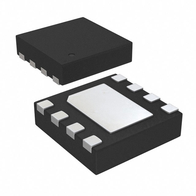
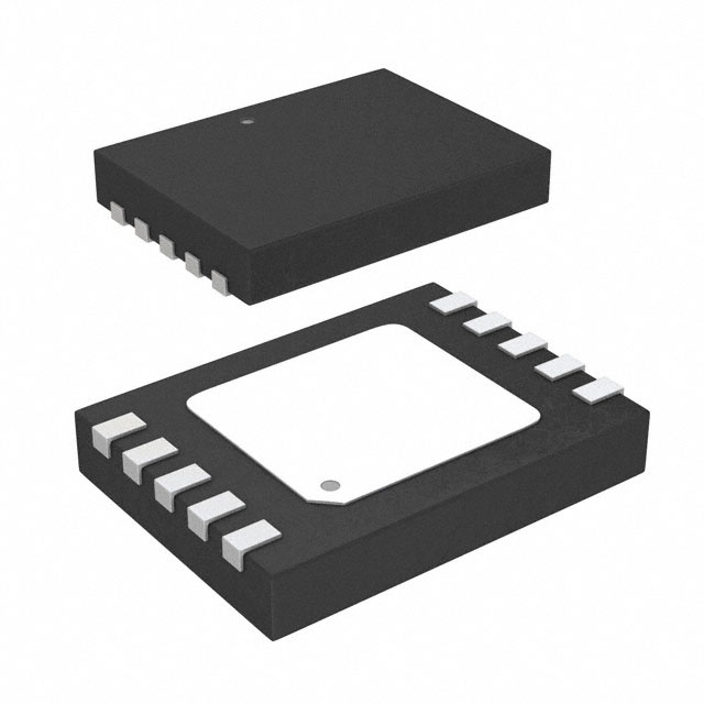
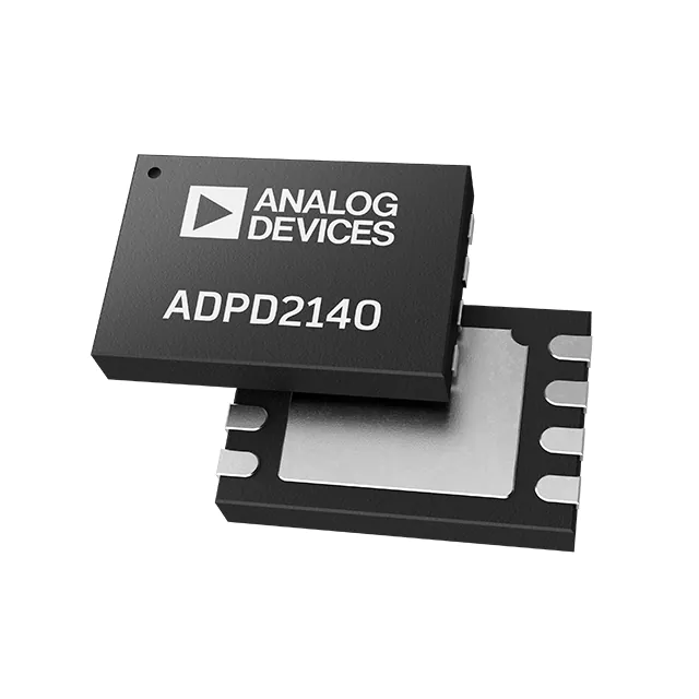
The ADP7185ACPZN0.5-R7 is a complementary metal oxide semiconductor(CMOS), low dropout (LDO) linear regulator that operatesfrom −2.0 V to −5.5 V and provides up to −500 mA of output current. This high output current LDO is ideal for regulation of high performance analog and mixed signal circuits operatingfrom −0.5 V down to −4.5 V. Using an advanced proprietaryarchitecture, the ADP7185ACPZN0.5-R7 provides high power supple rejectionratio (PSRR) and low noise, and it achieves excellent line and loadtransient response with a small 4.7 μF ceramic output capacitor.
The ADP7185ACPZN0.5-R7 is available in 15 fixed output voltage options.The following voltages are available from stock: −0.5 V, −1.0 V,−1.2 V, −1.5 V, −1.8 V, −2.0 V, −2.5 V, −3.0 V, and −3.3 V.
Additional voltages available by special order are −0.8 V, −0.9 V, −1.3 V, −2.8 V, −4.2 V, and −4.5 V. An adjustable version is also available which allows output voltages that range from −0.5 V to −VIN + 0.5 V with an external feedback divider.
The enable logic feature is capable of interfacing with positive or negative logic levels for maximum flexibility.
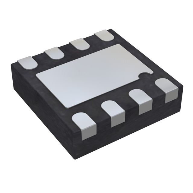
The ADP7185ACPZN0.5-R7 regulator output noise is 4 μV rms independent of the output voltage. The ADP7185ACPZN0.5-R7 is available in an 8-lead, 2 mm × 2 mm LFCSP, making it not only a very compact solution but also providing excellent thermal performance for applications requiring up to −500 mA of output current in a small, low profile footprint.
Feature
- Input voltage range: −2.0 V to −5.5 V
- Maximum output current: −500 mA
- Fixed output voltage options: −0.5 V to −4.5 V
- Adjustable output from −0.5 V to −VIN + 0.5 V
- Low output noise: 4 μV rms from 100 Hz to 100 kHz
- Noise spectral density: 20 nV/√Hz, 10 kHz to 1 MHz
- PSRR at −500 mA load
- 68 dB at 10 kHz
- 50 dB at 100 kHz
- 40 dB at 1 MHz
- Low dropout voltage: −190 mV typical at −500 mA load
- Initial output voltage (VOUT) accuracy: ±0.5%
- Output voltage accuracy over line, load, and temperature: ±2.2%
- Operating supply current (IGND): −0.6 mA typical at no load
- Low shutdown current: −2 μA typical at VIN = −5.5 V
- Stable with small 4.7 μF ceramic input and output capacitor
- Positive or negative enable logic
- Current-limit and thermal overload protection
- 8-lead, 2 mm × 2 mm LFCSP package
- Supported by ADIsimPOWER voltage regulator design tool
Applications
- Regulation to noise sensitive applications: analog-to-digital converters (ADCs), digital-to-analog converters (DACs), precision amplifiers
- Communications and infrastructure
- Medical and healthcare
- Industrial and instrumentation
(Picture: Pinout)

