The ADC requires a single 1.8 V power supply and LVPECL-/ CMOS-/LVDS-compatible sample rate clock for full performanceoperation. No external reference or driver components arerequired for many applications.
The ADC automatically multiplies the sample rate clock for theappropriate LVDS serial data rate. A data clock output (DCO) for capturing data on the output and a frame clock output (FCO) forsignaling a new output byte are provided. Individual channelpower-down is supported; the AD9645 typically consumes lessthan 2 mW in the full power-down state. The ADC providesseveral features designed to maximize flexibility and minimize system cost, such as programmable output clock and data alignment and digital test pattern generation. The available digital test patterns include built-in deterministic and pseudorandom patterns, along with custom user-defined test patterns entered via the serial port interface (SPI).
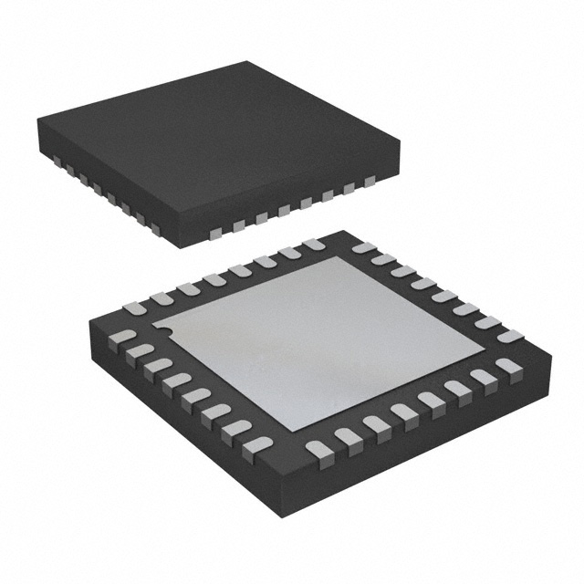
The AD9645 is available in a RoHS-compliant, 32-lead LFCSP. It is specified over the industrial temperature range of −40°C to +85°C. This product is protected by a U.S. patent.
PRODUCT HIGHLIGHTS
Feature
- 1.8 V supply operation
- Low power: 122 mW per channel at 125 MSPS with scalable power options
- SNR = 74 dBFS (to Nyquist)
- SFDR = 91 dBc at 70MHz
- DNL = ±0.65 LSB (typical); INL = ±1.5 LSB (typical)
- Serial LVDS (ANSI-644, default) and low power, reduced signal option (similar to IEEE 1596.3)
- 650 MHz full power analog bandwidth
- 2 V p-p input voltage range
- See data sheet for additional features
Applications
- Communications
- Diversity radio systems
- Multimode digital receiversGSM, EDGE, W-CDMA, LTE,CDMA2000, WiMAX, TD-SCDMA
- I/Q demodulation systems
- Smart antenna systems
- Broadband data applications
- Battery-powered instruments
- Hand held scope meters
- Portable medical imaging and ultrasound
- Radar/LIDAR
(Picture: Pinout)


