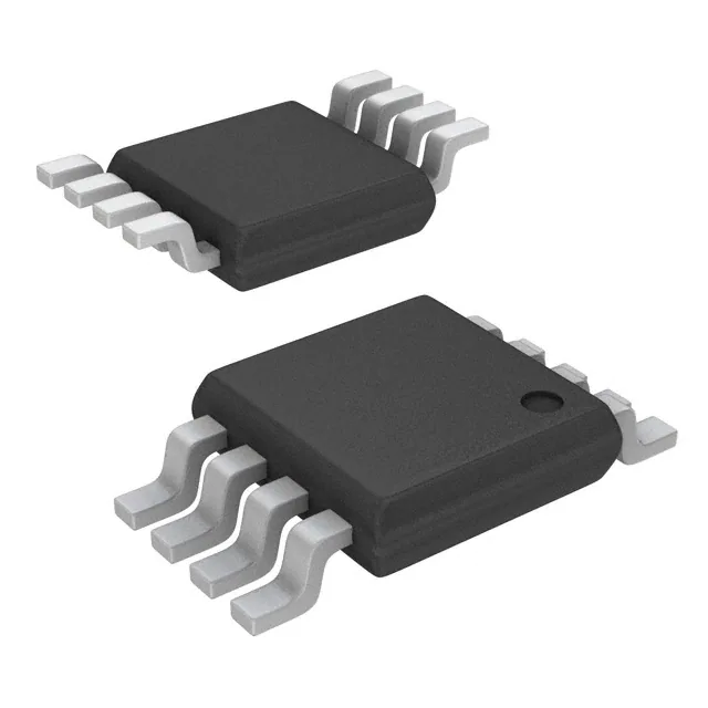
ADI's AD4000/AD4004/AD4008BCPZ-RL7 are low noise, low power, high speed, 16-bit, successive approximation register (SAR) analog-to-digital converters (ADCs) at 2 MSPS, 1 MSPS, and 500 kSPS, respectively. The high-Z mode coupled with a long acquisition phase eliminates the need for a dedicated high power, high-speed ADC driver, thus broadening the range of low power precision amplifiers that can drive this ADC directly while still achieving optimum performance. The input span compression feature enables the ADC driver amplifier and the ADC to operate off common supply rails without the need for a negative supply while preserving the full ADC code range. The low serial peripheral interface (SPI) clock rate requirement reduces the digital input/output power consumption, broadens processor options, and simplifies the task of sending data across digital isolation. Operating from a 1.8 V supply, these ADCs sample an analog input (IN+) between 0 V to VREF with respect to a ground sense (IN−) with VREF ranging from 2.4 V to 5.1 V.The reference voltage is applied externally and can be set independently of the supply voltage. The SPI-compatible versatile serial interface features seven different modes including the ability, using the SDI input, to daisy-chain several ADCs on a single 3-wire bus and provides an optional busy indicator. The AD4004 is compatible with 1.8 V, 2.5 V, 3 V, and 5 V logic, using the separate VIO supply. The AD4000/AD4004/AD4008BCPZ-RL7 are available in an MSOP or LFCSP with operation specified from -40°C to +125°C. The AD4000/AD4004/AD4008BCPZ-RL7 are ideal for medical equipment, machine automation, and battery-powered equipment applications.<strong>Features:</strong> 1 MSPS, 2 MSPS, INL: ±1.0 LSB maximum, Guaranteed 16-bit no missing codes, SNR: 93 dB typical at 1 kHz, 90 dB typical at 100 kHz, THD: -115 dB typical at 1 kHz, -95 dB typical at 100 kHz, Single 1.8 V supply operation with 1.71 V to 5.5 V logic interface, SAR architecture: no latency/pipeline delay, valid first conversion, Guaranteed operation: -40°C to +125°C, Serial interface SPI-/QSPI-/MICROWIRE-/DSP-compatible, Ability to daisy-chain multiple ADCs and provide a busy indicator, 10-lead packages: LFCSP, MSOP, Ease of use features reduce system power and complexity Input overvoltage clamp circuit, Reduced nonlinear input charge kickback, High-Z mode, Long acquisition phase, Input span compression, Fast conversion time allows low SPI clock rates, SPI-programmable modes, read/write capability, status word, Pseudo-differential (single-ended) analog input range 0 V to VREF with VREF between 2.4 V to 5.1 V
Feature
- Throughput: 2 MSPS/1 MSPS/500 kSPS options
- INL: ±1.0 LSB maximum
- Guaranteed 16-bit, no missing codes
- Low power
- 4.9 mW/MSPS, 2.5 mW at 500 kSPS, VDD only
- 7 mW/MSPS, 70 μW at 10 kSPS, 14 mW at 2 MSPS, total
- SNR: 93 dB typical at fIN = 1 kHz, 90 dB typical at fIN = 100 kHz
- Oversampled SNR
- 96 dB at 1.0 MSPS, OSR = 2
- 123 dB at 1.9 kSPS, OSR = 1024
- THD: −115 dB typical at fIN = 1 kHz, VREF = 5 V; −95 dB typical at fIN = 100 kHz
- SINAD: 82 dB at fIN = 1 MHz
- Easy Drive
- Greatly reduced input kickback
- Input current reduced to 0.4 μA/MSPS
- Long acquisition phase, ≥79% of cycle time at 1 MSPS
- Input span compression for single-supply operation
- Fast conversion time allows low SPI clock rates
- Input overvoltage clamp protection sinks up to 50 mA
- Pseudo differential input range
- 0 V to VREF with VREF from 2.4 V to 5.1 V
- Single 1.8 V supply operation with 1.71 V to 5.5 V logic interface
- First conversion accurate
- SPI-/QSPI-/MICROWIRE-/DSP-compatible serial interface
- Ability to daisy-chain multiple ADCs
- Guaranteed operation: −40°C to +125°C
- 10-lead packages: 3 mm × 3 mm LFCSP, 3 mm × 4.90 mm MSOP
- Pin compatible with AD4003/AD4007/AD4011 family
Applications
- Automatic test equipment
- Machine automation
- Medical equipment
- Battery-powered equipment
- Precision data acquisition systems
(Picture: Pinout)


