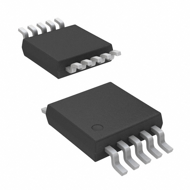
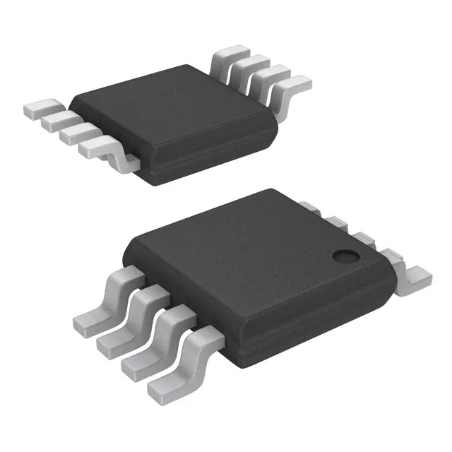
The AD5683R/AD5682R/AD5681R/AD5683, members of thenanoDAC+® family, are low power, single-channel, 16-/14-/12-bitbuffered voltage out digital-to-analog converters (DACs). Thedevices, except the AD5683, include an enabled by default internal2.5 V reference, offering 2 ppm/°C drift. The output span can beprogrammed to be 0 V to VREF or 0 V to 2 × VREF. All devicesoperate from a single 2.7 V to 5.5 V supply and are guaranteedmonotonic by design. The devices are available in a 2.00 mm ×2.00 mm, 8-lead LFCSP or a 10-lead MSOP.
The internal power-on reset circuit ensures that the DAC registeris written to zero scale at power-up while the internal outputbuffer is configured in normal mode. TheAD5683R/AD5682R/AD5681R/AD5683 contain a power-downmode that reduces the current consumption of the device to 2 µA(maximum) at 5 V and provides software selectable output loadswhile in power-down mode.
The AD5683R/AD5682R/AD5681R/AD5683 use a versatile3-wire serial interface that operates at clock rates of up to 50 MHz.Some devices also include asynchronous RESET pin and VLOGICpin options, allowing 1.8 V compatibility
Product Highlights
Feature
- Ultrasmall package: 2 mm × 2 mm, 8-lead LFCSP
- High relative accuracy (INL): ±2 LSB maximum at 16 bits
- AD5683R/AD5682R/AD5681R
- Low drift, 2.5 V reference: 2 ppm/°C typical
- Selectable span output: 2.5 V or 5 V
- Total unadjusted error (TUE): 0.06% of FSR maximum
- Offset error: ±1.5 mV maximum
- Gain error: ±0.05% of FSR maximum
- Low glitch: 0.1 nV-sec
- High drive capability: 20 mA
- Low power: 1.2 mW at 3.3 V
- Independent logic supply: 1.62 V logic compatible
- Wide operating temperature range: −40°C to +105°C
- Robust 4 kV HBM ESD protection
Applications
- Process controls
- Data acquisition systems
- Digital gain and offset adjustment
- Programmable voltage sources
(Picture: Pinout)


