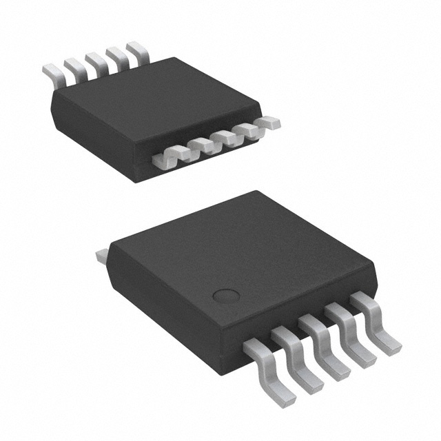
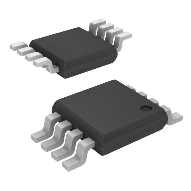
The AD5304/AD5314/AD5324BRM are quad 8-, 10-, and 12-bit buffered voltage output DACs in 10-lead MSOP and 10-lead LFCSP packages that operate from a single 2.5 V to 5.5 V supply, consuming 500 μA at 3 V. Their on-chip output amplifiers allow rail-to-rail output swing to be achieved with a slew rate of 0.7 V/μs. A 3-wire serial interface is used; it operates at clock rates up to 30 MHz and is compatible with standard SPI, QSPI, MICROWIRE, and DSP interface standards.
The references for the four DACs are derived from one reference pin. The outputs of all DACs can be updated simultaneously using the software LDAC function. The parts incorporate a power-on reset circuit, and ensure that the DAC outputs power up to 0 V and remains there until a valid write takes place to the device. The parts contain a power-down feature that reduces the current consumption of the device to 200 nA @ 5 V (80 nA @ 3 V).
The low power consumption of these parts in normal operation makes them ideally suited to portable battery-operated equipment. The power consumption is 3 mW at 5 V, 1.5 mW at 3 V, reducing to 1 μW in power-down mode.
Feature
- 4 buffered 12-Bit DACs in 10-lead MSOP and 10-lead LFCSP
- A, W Version: ±16 LSB INL, B Version: ±10 LSB INL
- Low power operation: 500μA @ 3V, 600μA @ 5V
- 2.5V to 5.5V power supply
- Guaranteed monotonic by design over all codes
- Power-down to 80nA @ 3V, 200nA @ 5V
- Double-buffered input logic
- Output range: 0V to VREF
- Power-on reset to 0V
- See data sheet for additional features
- Download(pdf)
- Military temperature range (−55°C to +125°C)
- Controlled manufacturing baseline
- One assembly/test site
- One fabrication site
- Enhanced product change notification
- Qualification data available on request
- V62/12628 DSCC Drawing Number
Applications
- Portable battery-powered instruments
- Digital gain and offset adjustment
- Programmable voltage and current sources
- Programmable attenuators
- Industrial process controls
(Picture: Pinout)


