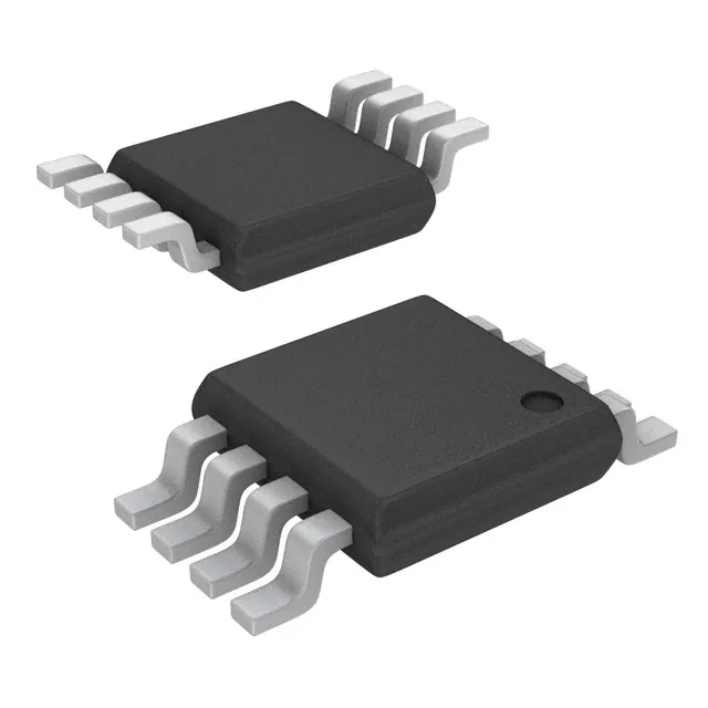
The AD5301/AD5311/AD5321BRM are single 8-/10-/12-bit, buffered,voltage-output DACs that operate from a single 2.5 V to5.5 V supply, consuming 120 μA at 3 V. The on-chip outputamplifier allows rail-to-rail output swing with a slew rate of0.7 V/μs. It uses a 2-wire (I2C-compatible) serial interface thatoperates at clock rates up to 400 kHz. Multiple devices can sharethe same bus.
The reference for the DAC is derived from the power supplyinputs and thus gives the widest dynamic output range. Thesedevices incorporate a power-on reset circuit, which ensures thatthe DAC output powers up to 0 V and remains there until avalid write takes place. The devices contain a power-downfeature that reduces the current consumption of the device to50 nA at 3 V and provides software-selectable output loadswhile in power-down mode.
The low power consumption in normal operation makes theseDACs ideally suited to portable battery-operated equipment. Thepower consumption is 0.75 mW at 5 V and 0.36 mW at 3 V,reducing to 1 μW in all power-down modes.
Feature
- Buffered voltage output 12-bit DAC
- 6-lead SOT-23 and 8-lead MSOP packages
- Micropower operation: 120 μA at 3 V
- 2-wire (I2C-compatible) serial interface
- Data readback capability
- 2.5 V to 5.5 V power supply
- Guaranteed monotonic by design over all codes
- Power-down to 50 nA at 3 V
- Reference derived from power supply
- Power-on reset to 0 V
- On-chip rail-to-rail output buffer amplifier
- 3 power-down functions
Applications
- Portable battery-powered instruments
- Digital gain and offset adjustment
- Programmable voltage and current sources
- Programmable attenuators
(Picture: Pinout)


