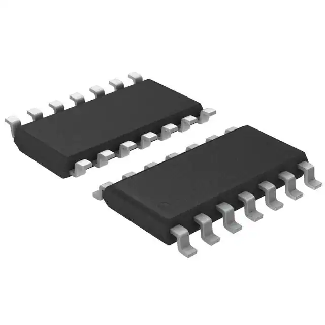
The MAX512/MAX513ESD contain three 8-bit, voltage-output digital-to-analog converters (DAC A, DAC B, and DAC C). Output buffer amplifiers for DACs A and B provide voltage outputs while reducing external component count. The output buffer for DAC A can source or sink 5mA to within 0.5V of VDD or VSS. The buffer for DAC B can source or sink 0.5mA to within 0.5V of VDD or VSS. DAC C is unbuffered, providing a third voltage output with increased accuracy. The MAX512 operates with a single +5V ±10% supply, and the MAX513ESD operates with a +2.7V to +3.6V supply. Both devices can also operate with split supplies. The 3-wire serial interface has a maximum operating frequency of 5MHz and is compatible with SPI, QSPI, and Microwire. The serial input shift register is 16 bits long and consists of 8 bits of DAC input data and 8 bits for DAC selection and shutdown. DAC registers can be loaded independently or in parallel at the positive edge of CS. A latched logic output is also available for auxiliary control. Ultra-low power consumption and small packages (14-pin DIP/SO) make the MAX512/MAX513ESD ideal for portable and battery-powered applications. Supply current is only 1mA, dropping to less than 1μA in shutdown. Any of the three DACs can be independently shut down. In shutdown mode, the DAC's R-2R ladder network is disconnected from the reference input, minimizing system power consumption.
Feature
- Operate from a Single +5V (MAX512) or +3V (MAX513) Supply, or from Bipolar Supplies
- Low Power Consumption
- 1mA Operating Current
- <1μA Shutdown Current
- Unipolar or Bipolar Outputs
- 5MHz, 3-Wire Serial Interface
- SPI, QSPI, and Microwire Compatible
- Two Buffered, Bipolar-Output DACs (DACs A/B)
- Independently Programmable Shutdown Mode
- Space-Saving 14-Pin SO/DIP Packages
- Pin and Software Reset
Applications
- Digital Gain and Offset Control
- Programmable Attenuators
- Programmable Current Sources
- Programmable Voltage Sources
- RF Digitally Adjustable Bias Circuits
- VCO Tuning


