The AD5544/AD5554 quad, 16-/14-bit, current output, digital-to-analog converters (DACs) are designed to operate from 2.7 V to 5.5 V supply range.
The applied external reference input voltage (VREFX) determines the full-scale output current. Integrated feedback resistors (RFB) provide temperature-tracking, full-scale voltage outputs when combined with an external I-to-V precision amplifier.
A double-buffered serial data interface offers high speed, 3-wire, SPI- and microcontroller-compatible inputs using serial data in (SDI), a chip select (CS), and clock (CLK) signals. In addition, a serial data out pin (SDO) allows for daisy-chaining when multiple packages are used. A common, level-sensitive, load DAC strobe (LDAC) input allows the simultaneous update of all DAC outputs from previously loaded input registers. Additionally, an internal power-on reset forces the output voltage to 0 at system turn-on. An MSB pin allows system reset assertion (RS) to force all registers to zero code when MSB = 0, or to half-scale code when MSB = 1.
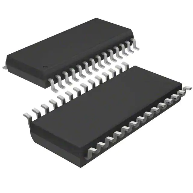
The AD5544ARS is packaged in the compact 28-lead SSOP and 32-lead LFCSP. The AD5554 is packaged in the compact 28-lead SSOP.
Feature
- 16-bit resolution INL of ±1 LSB (B Grade)
- 2 mA full-scale current ± 20%, with VREF = ±10 V
- 0.9 μs settling time to ±0.1%
- 12 MHz multiplying bandwidth
- Midscale glitch of −1 nV-sec
- Midscale or zero-scale reset
- Four separate, 4-quadrant multiplying reference inputs
- Compact 28-lead SSOP and 32-lead LFCSP
- See data sheet for additional features
- Download (pdf)
- Military temperature range (−55°C to +125°C)
- Controlled manufacturing baseline
- One assembly/test site
- One fabrication site
- Enhanced product change notification
- Qualification data available on request
- V62/12663 DSCC Drawing Number
Applications
- Automatic test equipment
- Instrumentation
- Digitally controlled calibration
(Picture: Pinout)


