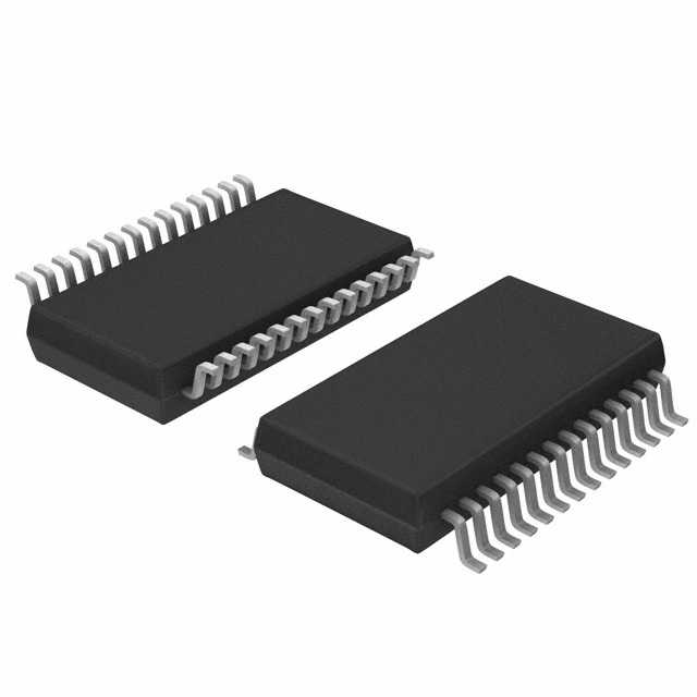
The MAX5180BEEI contains two 10-bit, simultaneous-update, current-output digital-to-analog converters (DACs) designed for superior performance in communications systems requiring analog signal reconstruction with low distortion and low-power operation. The MAX5183 provides equal specifications, with on-chip precision resistors for voltage output operation. The devices are designed for 10pV-s glitch operation to minimize unwanted spurious signal components at the output. An on-board 1.2V bandgap circuit provides a well-regulated, low-noise reference that can be disabled for external reference operation. The MAX5180/MAX5183 are designed to provide a high level of signal integrity for the least amount of power dissipation. The DACs operate from a single supply of 2.7V to 3.3V. Additionally, these DACs have three modes of operation: normal, low-power standby, and complete shutdown, which provides the lowest possible power dissipation with 1μA (max) shutdown current. A fast wake-up time (0.5μs) from standby mode to full DAC operation conserves power by activating the DACs only when required. The MAX5180/MAX5183 are packaged in a 28-pin QSOP and are specified for the extended (-40°C to +85°C) temperature range. For lower-resolution, dual 8-bit versions, refer to the MAX5186/MAX5189 data sheet.
Feature
- 2.7V to 3.3V Single-Supply Operation
- Wide Spurious-Free Dynamic Range: 70dB at fOUT = 2.2MHz
- Fully Differential Outputs for Each DAC
- ±0.5% FSR Gain Mismatch
- ±0.2° Phase Mismatch
- Low-Current Standby or Full-Shutdown Modes
- Internal 1.2V Low-Noise Bandgap Reference
- Small 28-Pin QSOP Package
Applications
- Arbitrary Waveform Generation (AWG)
- Digital Signal Processing (DSP)
- Imaging
- Signal Reconstruction of I and Q Transmit
- Signals


