The AD5620/AD5640/AD5660-1 parts include an internal, 1.25 V, 5 ppm/°C reference, giving a full-scale output voltage range of 2.5 V. The AD5620/AD5640/AD5660-2-3 parts include an internal, 2.5 V, 5 ppm/°C reference, giving a full-scale output voltage range of 5 V. The reference associated with each part is available at the VREFOUT pin.
The parts incorporate a power-on reset circuit to ensure that the DAC output powers up to 0 V (AD5620/AD5640/AD5660-1-2) or midscale (AD5620-3 and AD5660-3) and remains there until a valid write takes place. The parts contain a power-down feature that reduces the current consumption of the device to 480 nA at 5 V and provides software-selectable output loads while in power-down mode. The power consumption is 2.5 mW at 5 V, reducing to 1 μW in power-down mode.
The AD5620/AD5640/AD5660 on-chip precision output amplifier allows rail-to-rail output swing to be achieved. For remote sensing applications, the output amplifier’s inverting input is available to the user. The AD5620/AD5640/AD5660 use a versatile 3-wire serial interface that operates at clock rates up to 30 MHz and is compatible with standard SPI®, QSPI™, MICROWIRE™, and DSP interface standards.
Product Highlights
Feature
- 12-Bit DAC; 12-Bit Accuracy Guaranteed
- On-chip, 1.25 V/2.5 V, 5 ppm/°C reference
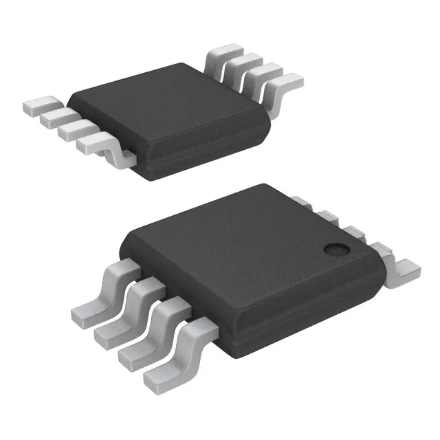
- Tiny 8-lead SOT-23/MSOP packages
- Power-down to 480 nA @ 5 V, 200 nA @ 3 V
- 3 V/5 V single power supply
- Guaranteed 16-bit monotonic by design
- Power-on reset to zero/midscale
- 3 power-down functions
- Serial interface with Schmitt-triggered inputs
- Rail-to-rail operation
- SYNC interrupt facility
Applications
- Process control
- Data acquisition systems
- Portable battery-powered instruments
- Digital gain and offset adjustment
- Programmable voltage and current sources
- Programmable attenuators
(Picture: Pinout)


