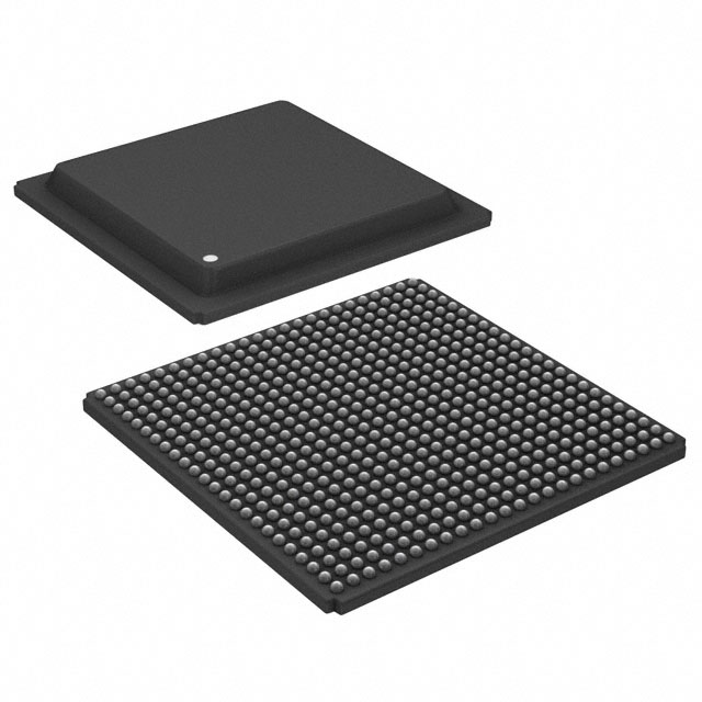
The ADSP-TS201S TigerSHARC processor is an ultrahigh performance, static superscalar processor optimized for large signal processing tasks and communications infrastructure. The DSP combines very wide memory widths with dual computation blocks—supporting floating-point (IEEE 32-bit and extended precision 40-bit) and fixed-point (8-, 16-, 32-, and 64-bit) processing—to set a new standard of performance for digital signal processors. The TigerSHARC static superscalar architecture lets the DSP execute up to four instructions each cycle, performing 24 fixed-point (16-bit) operations or six floating-point operations.
Four independent 128-bit wide internal data buses, each connecting to the six 4M bit memory banks, enable quad-word data, instruction, and I/O access and provide 33.6G bytes per second of internal memory bandwidth. Operating at 600 MHz, the ADSP-TS201S processor’s core has a 1.67 ns instruction cycle time. Using its single-instruction, multiple-data (SIMD) features, the ADSP-TS201S processor can perform 4.8 billion, 40-bit MACS or 1.2 billion, 80-bit MACS per second.
The ADSP-TS201S processor is code compatible with the other TigerSHARC processors.
The Functional Block Diagram on Page 1 shows the ADSP-TS201S processor’s architectural blocks. These blocks include:
• Dual compute blocks, each consisting of an ALU, multiplier, 64-bit shifter, 128-bit CLU, and 32-word register file and associated data alignment buffers (DABs)
• Dual integer ALUs (IALUs), each with its own 31-word register file for data addressing and a status register
• A program sequencer with instruction alignment buffer (IAB) and branch target buffer (BTB)
• An interrupt controller that supports hardware and software interrupts, supports level- or edge-triggers, and supports prioritized, nested interrupts
• Four 128-bit internal data buses, each connecting to the six 4M bit memory banks
• On-chip DRAM (24M bit)
• An external port that provides the interface to host processors, multiprocessing space (DSPs), off-chip memorymapped peripherals, and external SRAM and SDRAM
• A 14-channel DMA controller
• Four full-duplex LVDS link ports
• Two 64-bit interval timers and timer expired pin
• An 1149.1 IEEE-compliant JTAG test access port for onchip emulation
KEY FEATURES
Up to 600 MHz, 1.67 ns instruction cycle rate 24M bits of internal—on-chip—DRAM memory25 mm × 25 mm (576-ball) thermally enhanced ball grid array package
Dual-computation blocks—each containing an ALU, a
multiplier, a shifter, a register file, and a communications logic unit (CLU)
Dual-integer ALUs, providing data addressing and pointer manipulation
Integrated I/O includes 14-channel DMA controller, external
port, four link ports, SDRAM controller, programmable
flag pins, two timers, and timer expired pin for system integration
KEY BENEFITS
Provides high performance static superscalar DSP
operations, optimized for telecommunications
infrastructure and other large, demanding multiprocessor DSP applications
Performs exceptionally well on DSP algorithm and I/O
benchmarks (see benchmarks in Table 1)
Supports low overhead DMA transfers between internal
memory, external memory, memory-mapped peripherals,
link ports, host processors, and other (multiprocessor) DSPs
Eases DSP programming through extremely flexible instruction set and high-level-language-friendly DSP architecture
Enables scalable multiprocessing systems with low communications overhead
Provides on-chip arbitration for glueless multiprocessing
Single-precision IEEE 32-bit and extended-precision 40-bit
floating-point data formats and 8-, 16-, 32-, and 64-bit fixed-point data formats
The TigerSHARC DSP uses a Static SuperscalarTM† architecture. This architecture is superscalar in that the ADSP-TS201S processor’s core can execute simultaneously from one to four 32-bit instructions encoded in a very large instruction word (VLIW) instruction line using the DSP’s dual compute blocks. Because the DSP does not perform instruction re-ordering at runtime— the programmer selects which operations will execute in parallel prior to runtime—the order of instructions is static. With few exceptions, an instruction line, whether it contains one, two, three, or four 32-bit instructions, executes with a throughput of one cycle in a 10-deep processor pipeline.
For optimal DSP program execution, programmers must follow the DSP’s set of instruction parallelism rules when encoding an instruction line. In general, the selection of instructions that the DSP can execute in parallel each cycle depends on the instruction line resources each instruction requires and on the source and destination registers used in the instructions. The programmer has direct control of three core components—the IALUs, the compute blocks, and the program sequencer.
The ADSP-TS201S processor, in most cases, has a two-cycle execution pipeline that is fully interlocked, so—whenever a computation result is unavailable for another operation dependent on it—the DSP automatically inserts one or more stall cycles as needed. Efficient programming with dependency-free instructions can eliminate most computational and memory transfer data dependencies.
In addition, the ADSP-TS201S processor supports SIMD operations two ways—SIMD compute blocks and SIMD computations. The programmer can load both compute blocks with the same data (broadcast distribution) or different data (merged distribution).


