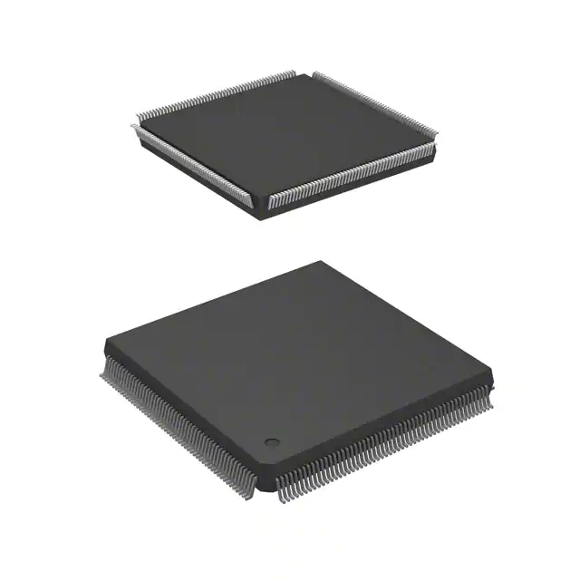
Microsemi's 42MX families offer a cost-effective design solution at 5V. The MX devices are single-chip solutions and provide high performance while shortening the system design and development cycle. MX devices can integrate and consolidate logic implemented in multiple PALs, CPLDs, and FPGAs. Example applications include high-speed controllers and address decoding, peripheral bus interfaces, DSP, and co-processor functions.
The MX device architecture is based on Microsemi’s patented antifuse technology implemented in a 0.45µm triple-metal CMOS process. With capacities ranging from 3,000 to 54,000 system gates, the MX devices provide performance up to 250 MHz, are live on power-up and have one-fifth the standby power consumption of comparable FPGAs. MX FPGAs provide up to 202 user I/Os and are available in a wide variety of packages and speed grades. A42MX24 and A42MX36 devices also feature MultiPlex I/Os, which support mixed-voltage systems, enable programmable PCI, deliver high-performance operation at both 5.0V and 3.3V, and provide a lowpower mode. The devices are fully compliant with the PCI Local Bus Specification (version 2.1). They deliver 200 MHz on-chip operation and 6.1 ns clock-to-output performance.
All MX devices are fully tested over automotive and military temperature ranges. In addition, the largest member of the family, the A42MX36, is available in both CQ208 and CQ256 ceramic packages screened to MIL-STD-883 levels. For easy prototyping and conversion from plastic to ceramic, the CQ208 and PQ208 devices are pin-compatible.
Feature
High Capacity
• Single-Chip ASIC Alternative
• 3,000 to 54,000 System Gates
• Up to 2.5 kbits Configurable Dual-Port SRAM
• Fast Wide-Decode Circuitry
• Up to 202 User-Programmable I/O Pins
High Performance
• 5.6 ns Clock-to-Out
• 250 MHz Performance
• 5 ns Dual-Port SRAM Access
• 100 MHz FIFOs
• 7.5 ns 35-Bit Address Decode
HiRel Features
• Commercial, Industrial, Automotive, and Military Temperature Plastic Packages
• Commercial, Military Temperature, and MIL-STD-883 Ceramic Packages
• QML Certification
• Ceramic Devices Available to DSCC SMD
Ease of Integration
• Mixed-Voltage Operation (5.0 V or 3.3 V for core and
I/Os), with PCI-Compliant I/Os
• Up to 100% Resource Utilization and 100% Pin Locking
• Deterministic, User-Controllable Timing
• Unique In-System Diagnostic and Verification Capability with Silicon Explorer II
• Low Power Consumption
• IEEE Standard 1149.1 (JTAG) Boundary Scan Testing

