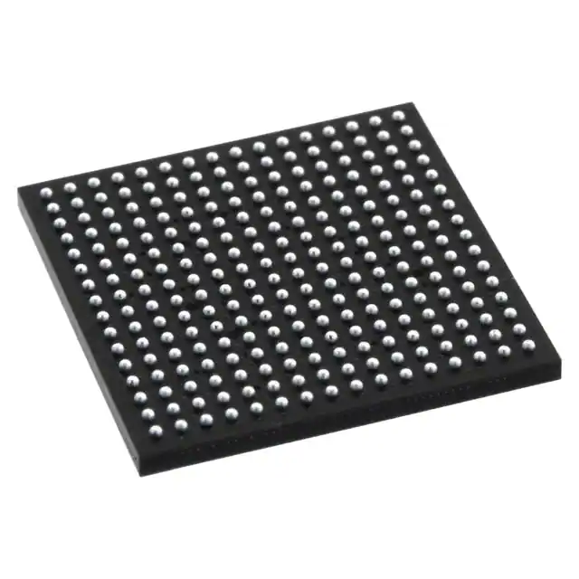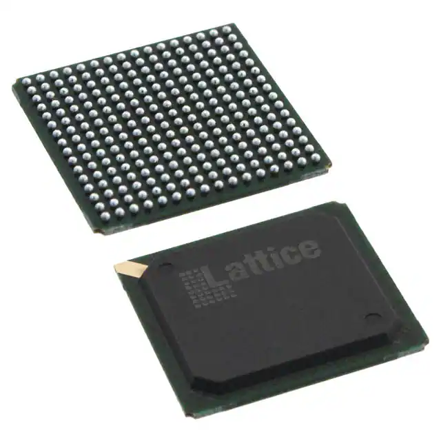
The LatticeXP family of FPGA devices combine logic gates, embedded memory and high performance I/Os in a single architecture that is both non-volatile and infinitely reconfigurable to support cost-effective system designs.
The re-programmable non-volatile technology used in the LatticeXP family is the next generation ispXP™ technology. With this technology, expensive external configuration memories are not required and designs are secured from unauthorized read-back. In addition, instant-on capability allows for easy interfacing in many applications.
The ispLEVER® design tool from Lattice allows large complex designs to be efficiently implemented using the LatticeXP family of FPGA devices. Synthesis library support for LatticeXP is available for popular logic synthesis tools. The ispLEVER tool uses the synthesis tool output along with the constraints from its floor planning tools to place and route the design in the LatticeXP device. The ispLEVER tool extracts the timing from the routing and backannotates it into the design for timing verification.
Lattice provides many pre-designed IP (Intellectual Property) ispLeverCORE™ modules for the LatticeXP family. By using these IPs as standardized blocks, designers are free to concentrate on the unique aspects of their design, increasing their productivity.
Feature
■ Non-volatile, Infinitely Reconfigurable
• Instant-on
– powers up in microseconds
• No external configuration memory
• Excellent design security, no bit stream to intercept
• Reconfigure SRAM based logic in milliseconds
• SRAM and non-volatile memory programmable through system configuration and JTAG ports
■ Sleep Mode
• Allows up to 1000x static current reduction
■ TransFR™ Reconfiguration (TFR)
• In-field logic update while system operates
■ Extensive Density and Package Options
• 3.1K to 19.7K LUT4s
• 62 to 340 I/Os
• Density migration supported
■ Embedded and Distributed Memory
• 54 Kbits to 396 Kbits sysMEM™ Embedded Block RAM
• Up to 79 Kbits distributed RAM
• Flexible memory resources: − Distributed and block memory
■ Flexible I/O Buffer
• Programmable sysIO™ buffer supports wide range of interfaces:
− LVCMOS 3.3/2.5/1.8/1.5/1.2
− LVTTL
– SSTL 18 Class I
− SSTL 3/2 Class I, II
– HSTL15 Class I, III
− HSTL 18 Class I, II, III
− PCI
− LVDS, Bus-LVDS, LVPECL, RSDS
■ Dedicated DDR Memory Support
• Implements interface up to DDR333 (166MHz)
■ sysCLOCK™ PLLs
• Up to 4 analog PLLs per device
• Clock multiply, divide and phase shifting
■ System Level Support
• IEEE Standard 1149.1 Boundary Scan, plus ispTRACY™ internal logic analyzer capability
• Onboard oscillator for configuration
• Devices operate with 3.3V, 2.5V, 1.8V or 1.2V power supply