久芯网

LFXP2-8E-7QN208C

  • 描述:电源电压: 1.14伏~1.26伏 供应商设备包装: 208-PQFP(28x28) 工作温度: 0摄氏度~85摄氏度(TJ) 安装类别: 表面安装
  • 品牌: 莱迪思 (Lattice)
  • 交期:5-7 工作日
渠道:
  • 自营
  • 得捷
  • 贸泽

起订量: 24

  • 库存: 0
  • 单价: ¥379.52796
  • 数量:
    - +
  • 总计: ¥9,108.67
在线询价

温馨提示: 请填写以下信息,以便客户代表及时与您沟通联系。

规格参数

  • 制造厂商 莱迪思 (Lattice)
  • 部件状态 可供货
  • 闸门数量 -
  • 安装类别 表面安装
  • 工作温度 0摄氏度~85摄氏度(TJ)
  • 包装/外壳 208亿qfp
  • 供应商设备包装 208-PQFP(28x28)
  • 电源电压 1.14伏~1.26伏
  • 逻辑阵列块/可配置逻辑块数量 one thousand
  • RAM 总位数 226304
  • 逻辑元件/单元的数量 8000
  • 输入/输出数量 146

LFXP2-8E-7QN208C 产品详情

Lattice's��LatticeXP2��non-volatile��field programmable gate arrayscombine a look-up table-based��FPGA��fabric with Flash non-volatile cells in a��flexiFlash��⒙�architecture. The��flexiFlash��architecture provides instant-on, small footprint, on-chip storage with��FlashBAK��⒙�embedded block memories, Serial TAG memory, and design security. The devices include LUT-based logic, distributed and embedded memory, Phase Locked Loops, pre-engineered source synchronous I/O, and enhanced sysDSP blocks. The product is ideal for high-volume, low-cost applications.

Feature

 flexiFLASH™ Architecture 

• Instant-on 

• Infinitely reconfigurable 

• Single chip 

• FlashBAK™ technology 

• Serial TAG memory 

• Design security 

 Live Update Technology 

• TransFR™ technology 

• Secure updates with 128 bit AES encryption 

• Dual-boot with external SPI 

 sysDSP™ Block 

• Three to eight blocks for high performance Multiply and Accumulate 

• 12 to 32 18x18 multipliers 

• Each block supports one 36x36 multiplier or four 18x18 or eight 9x9 multipliers 

 Embedded and Distributed Memory 

• Up to 885 Kbits sysMEM™ EBR 

• Up to 83 Kbits Distributed RAM 

 sysCLOCK™ PLLs 

• Up to four analog PLLs per device 

• Clock multiply, divide and phase shifting

 Flexible I/O Buffer 

• sysIO™ buffer supports: 

– LVCMOS 33/25/18/15/12; LVTTL 

– SSTL 33/25/18 class I, II 

– HSTL15 class I; HSTL18 class I, II 

– PCI 

– LVDS, Bus-LVDS, MLVDS, LVPECL, RSDS 

 Pre-engineered Source Synchronous Interfaces 

• DDR / DDR2 interfaces up to 200 MHz 

• 7:1 LVDS interfaces support display applications 

• XGMII 

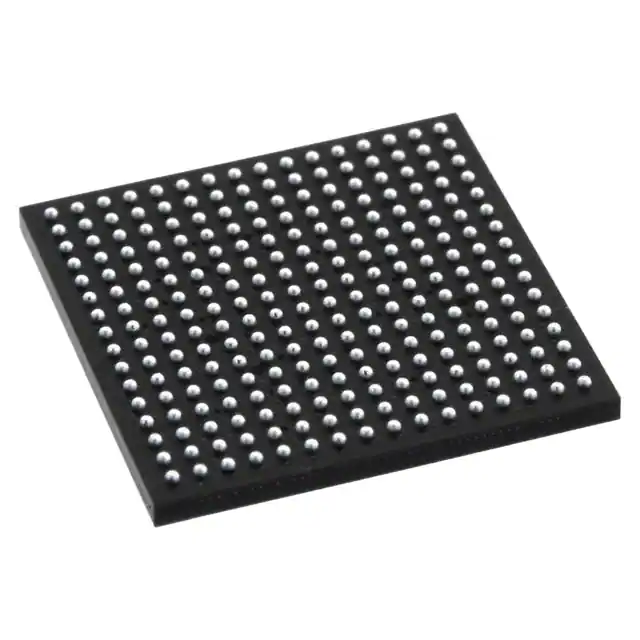
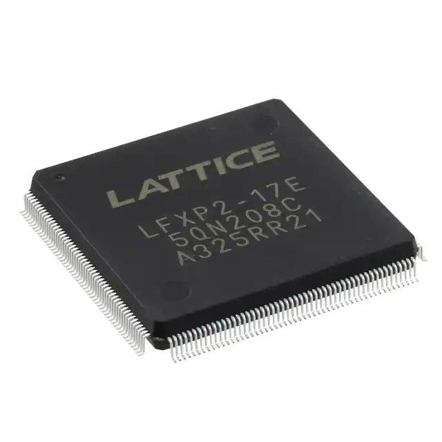
 Density And Package Options 

• 5k to 40k LUT4s, 86 to 540 I/Os 

• csBGA, TQFP, PQFP, ftBGA and fpBGA packages 

• Density migration supported 

 Flexible Device Configuration 

• SPI (master and slave) Boot Flash Interface 

• Dual Boot Image supported 

• Soft Error Detect (SED) macro embedded 

 System Level Support 

• IEEE 1149.1 and IEEE 1532 Compliant 

• On-chip oscillator for initialization & general use 

• Devices operate with 1.2V power supply


LFXP2-8E-7QN208C所属分类:现场可编程门阵列(FPGA),LFXP2-8E-7QN208C 由 莱迪思 (Lattice) 设计生产,可通过久芯网进行购买。LFXP2-8E-7QN208C价格参考¥379.527960,你可以下载 LFXP2-8E-7QN208C中文资料、PDF数据手册、Datasheet数据手册功能说明书,可查询LFXP2-8E-7QN208C规格参数、现货库存、封装信息等信息!

莱迪思 (Lattice)

莱迪思 (Lattice)

莱迪思半导体是低功耗可编程的领导者。在不断增长的通信、计算、工业、汽车和消费市场中,他们通过网络解决客户问题,从边缘到云。他们的技术、长期关系以及对世界一流支持的承诺,让他们的客户能够快速、轻松地释放他...

展开
会员中心 微信客服
客服
回到顶部