The devices operate from an on-chip oscillator and a PLL generating an internal high frequency clock of 41.78 MHz. This clock is routed through a programmable clock divider from which the MCU core clock operating frequency is generated. The microcontroller core is an ARM7TDMI®, 16-bit/32-bit RISC machine, which offers up to 41 MIPS peak performance. Thirty-two kilobytes of SRAM and 126 kB of nonvolatile Flash/EE memory are provided on-chip. The ARM7TDMI core views all memory and registers as a single linear array.
The ADuC7124 contains an advanced interrupt controller. The vectored interrupt controller (VIC) allows every interrupt to be assigned a priority level. It also supports nested interrupts to a maximum level of eight per IRQ and FIQ. When IRQ and FIQ interrupt sources are combined, a total of 16 nested interrupt levels are supported.On-chip factory firmware supports in-circuit download via the UART serial interface port or the I2C port, while nonintrusive emulation is also supported via the JTAG interface. These features are incorporated into a low cost QuickStart™ Development System supporting this MicroConverter® family.The part contains a 16-bit PWM with six output signals.For communication purposes, the part contains 2× I2C channels that can be individually configured for Master or Slave mode. An SPI interface supporting both master and slave modes is also provided. Thirdly, 2× UART channels are provided. Each UART contains a configurable 16-bit FIFO with the receive and transmit buffers.
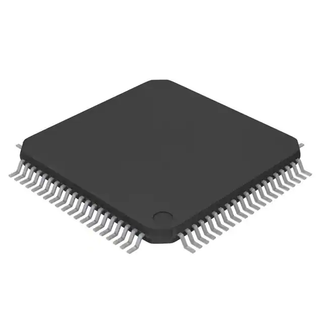
The parts operate from 2.7 V to 3.6 V and are specified over an industrial temperature range of −40°C to +125°C. When operating at 41.78 MHz, the power dissipation is typically 120 mW. The ADuC7124 is available in either 64-lead LFCSP or 80-lead LFQFP packages.
Applications- Industrial control and automation systems
- Smart sensors, precision instrumentation
- Base station systems, optical networking
- Patient monitoring
Feature
- Multichannel, 12-bit, 1 MSPS ADCUp to 16 ADC channels
- Fully differential and single-ended modes
- 0 V to VREF analog input range
- 12-bit voltage output DACsUp to 4 DAC outputs available
- On-chip voltage reference
- On-chip temperature sensor (±3°C)
- Voltage comparator
- ARM7TDMI core, 16-bit/32-bit RISC architecture
- JTAG port supports code download and debug
- Trimmed on-chip oscillator (±3%)
- External watch crystal
- External clock source up to 44 MHz
- See data sheet for additional features
Applications
- Industrial control and automation systems
- Smart sensors, precision instrumentation
- Base station systems, optical networking
- Patient monitoring


