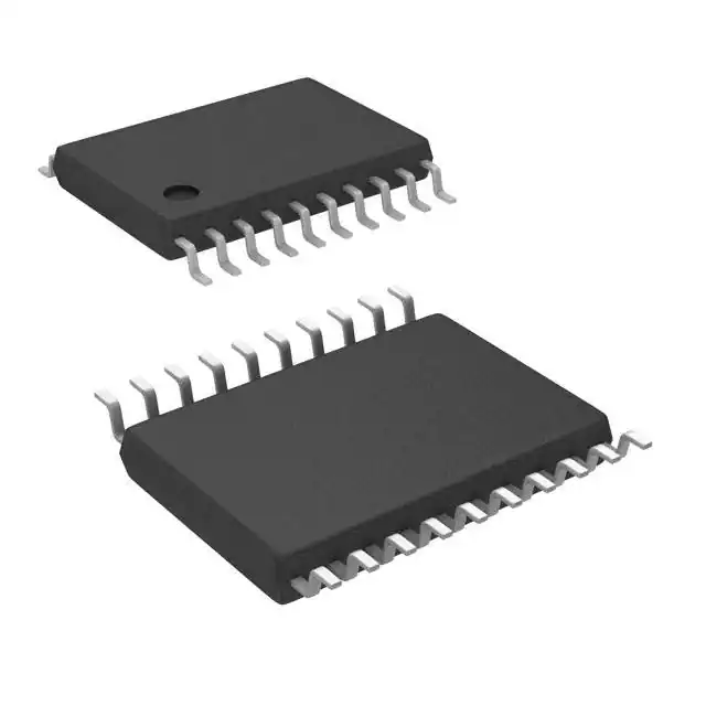
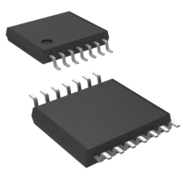
The ADG451BN is a monolithic CMOS device comprising four independently selectable switches. It is designed on an enhanced LC2MOS process which provides low power dissipation yet gives high switching speed and low on resistance.
The ADG451BN switches are turned on with a logic low on the appropriate control input. Each switch conducts equally well in both directions when ON and each has an input signal range that extends to the supplies. All switches exhibit break-before-make switching action for use in multiplexer applications. Inherent in the design is low charge injection for minimum transients when switching the digital inputs.
Feature
- Low On-Resistance (4 Ω)
- On-Resistance Flatness 0.2 Ω
- 44 V Supply Maximum Ratings
- ± 15 V Analog Signal Range
- Fully Specified @ ±5V, +12V, ±15V
- Ultralow Power Dissipation (18 µW)
- ESD 2 kV
- Continuous Current 100mA
- Fast Switching Times ton < 70 nstoff < 60 ns
- TTL/CMOS-Compatible Inputs
Applications
- Relay Replacement
- Audio and Video Switching
- Automatic Test Equipment
- Precision Data Acquisition
- Battery-Powered Systems
- Sample Hold Systems
- Communication Systems
- PBX, PABX Systems
- Avionics
(Picture: Pinout)


