The ADG508AKP and ADG509A are designed on an enhanced LC2MOS process that gives an increased signal capability of VSS to VDD and enables operation over a wide range of supply voltages. The devices can comfortably operate anywhere in the 10.8 V to 16.5 V single- or dual-supply range. These multiplexers also feature high switching speeds and low RON.
Product Highlights
- Single-/Dual-Supply Specifications with a Wide Tolerance. The devices are specified in the 10.8 V to 16.5 V range for both single and dual supplies.
- Extended Signal Range. The enhanced LC2MOS processing results in a high breakdown and an increased analog signal range of VSS to VDD.
- Break-Before-Make Switching. Switches are guaranteed break-before-make so that input signals are protected against momentary shorting.
- Low Leakage. Leakage currents in the range of 20 pA make these multiplexers suitable for high precision circuits.
Feature
- 44 V supply maximum rating
- VSS to VDD analog signal range
- Single-/dual-supply specifications
- Wide supply range: 10.8 V to 16.5 V
- Extended plastic temperature range: −40°C to +85°C
- Low power dissipation: 28 mW maximum
- Low leakage: 20 pA typical
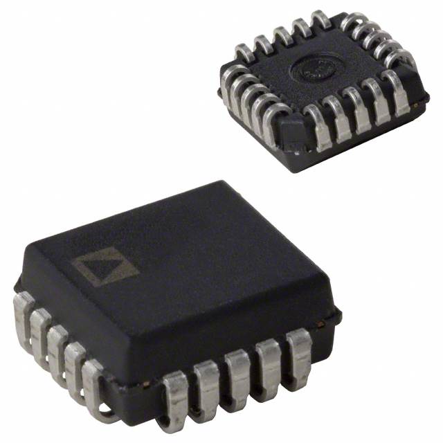
- Available in 16-lead DIP/SOIC and 20-lead PLCC/LCC packages
- Superior alternative toDG508A, HI-508DG509A, HI-509
(Picture: Pinout)


