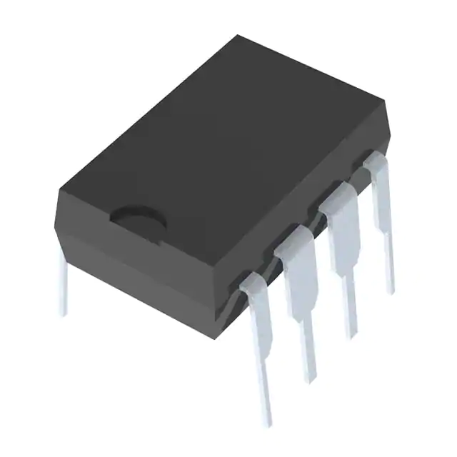
The ADM485JNZ operates from a single +5 V power supply.Excessive power dissipation caused by bus contention or by output shorting is prevented by a thermal shutdown circuit.This feature forces the driver output into a high impedance state if during fault conditions a significant temperature increase is detected in the internal driver circuitry.
Up to 32 transceivers may be connected simultaneously on a bus, but only one driver should be enabled at any time.It is important, therefore, that the remaining disabled drivers do not load the bus.To ensure this, the ADM485JNZ driver features high output impedance when disabled and also when powered down.
This minimizes the loading effect when the transceiver is not being utilized.The high impedance driver output is maintained over the entire common-mode voltage range form -7V to +12 V.
The receiver contains a fail safe feature which results in a logic high output state if the inputs are unconnected (floating).
The ADM485JNZ is fabricated on BiCMOS, an advanced mixed technology process combining low power CMOS with fast switching bipolar technology.All inputs and outputs contain protection against EDS; all diver outputs feature high source and sink current capability.An epitaxial layer is used to guard against latch-up.
The ADM485JNZ features extremely fast switching speeds.Minimal driver propagation delays permit transmission at data rates up to 5 Mbits/s while low skew minimizes EMI interference.
The part is fully specified over the commercial and industrial temperature range and is available in an 8-pin DIL/SOIC packages.
Feature
- Meets EIA RS-485 Standard
- 5 Mbps Data Rate
- Single 5 V Supply
- –7 V to +12 V Bus Common-Mode Range
- High Speed, Low Power BiCMOS
- Thermal Shutdown Protection
- Short-Circuit Protection
- Driver Propagation Delay: 10 ns
- Receiver Propagation Delay: 15 ns
- High Z Outputs with Power Off
- Superior Upgrade for LTC485


