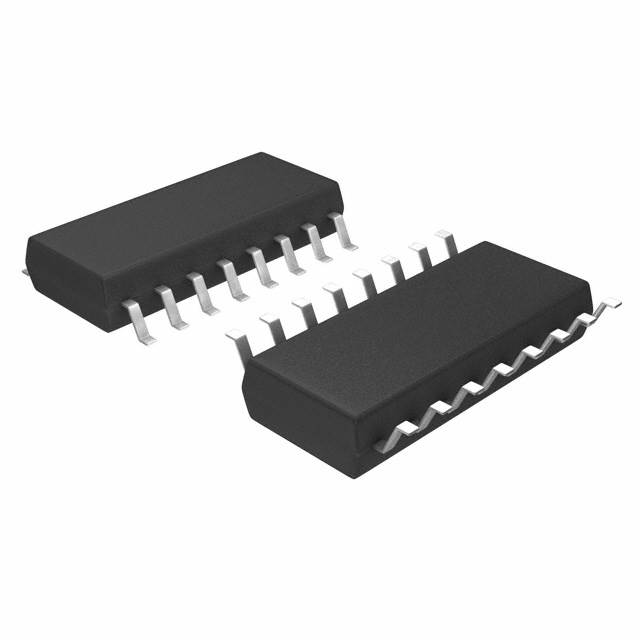
1. AM26LS32ACNSR Devices Meet or Exceed the Requirements of ANSI TIA/EIA-422-B, TIA/EIA-423-B, and ITU Recommendations V.10 and V.11
2. AM26LS32ACNSR Devices Have ±7-V Common-Mode Range With ±200-mV Sensitivity 3.AM26LS33A Devices Have ±15-V Common-Mode Range With ±500-mV Sensitivity
4. Input Hysteresis . . . 50 mV Typical
5. Operate From a Single 5-V Supply
6. Low-Power Schottky Circuitry
7. 3-State Outputs
8. Complementary Output-Enable Inputs
9. Input Impedance . . . 12 k Minimum
10. Designed to Be Interchangeable With Advanced Micro Devices AM26LS32 and AM26LS33Description :The AM26LS32ACNSR and AM26LS33A devices are s for balanced and unbalanced digital data transmission. The enable function is common to all four receivers and offers a choice of active-high or active-low input. The 3-state outputs permit connection directly to a bus-organized system. Fail-safe design ensures that, if the inputs are open, the outputs always are high. Compared to the AM26LS32 and the AM26LS33, the AM26LS32ACNSR and AM26LS33A incorporate an additional stage of amplification to improve sensitivity. The input impedance has been increased, resulting in less loading of the bus line. The additional stage has increased propagation delay; however, this does not affect interchangeability in most applications. The AM26LS32AC and AM26LS33AC are characterized for operation from 0°C to 70°C. The AM26LS32AI is characterized for operation from –40°C to 85°C. The AM26LS32AM and AM26LS33AM are characterized for operation over the full military temperature range of –55°C to 125°C.


