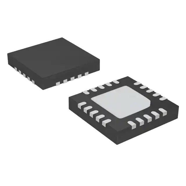
The SN65HVD101 and ‘HVD102 IO-Link PHYs implement the IO-Link interface for industrialpoint-to-point communication. When the device is connected to an IO-Link master through a 3-wireinterface, the master can initiate communication and exchange data with the remote node while theSN65HVD10X acts as a complete physical layer for the communication.
The IO-Link driver output (CQ) can be used in push-pull, high-side, or low-sideconfigurations using the EN and TX input pins. The PHY receiver converts the 24-V IO-Link signal onthe CQ pin to standard logic levels on the RX pin. A simple parallel interface is used to receiveand transmit data and status information between the PHY and the local controller.
The SN65HVD101 and ’HVD102 implement protection features forovercurrent, overvoltage and overtemperature conditions. The IO-Link driver current limit can beset using an external resistor. If a short-circuit current fault occurs, the driver outputs areinternally limited, and the PHY generates an error signal (SC). These devices also implement anovertemperature shutdown feature that protects the device from high-temperature faults.
The SN65HVD102RGBT operates from a single external 3.3-V or 5-V local supply. The SN65HVD101integrates a linear regulator that generates either 3.3 V or 5 V from the IO-Link L+ voltage forsupplying power to the PHY as well as a local controller and additional circuits.
The SN65HVD101 and ’HVD102 are available in the 20-pin RGB package (4 mm × 3,5 mm QFN)for space-constrained applications.
Feature
- Configurable CQ Output: Push-Pull, High-Side, or Low-Side for SIO Mode
- Remote Wake-Up Indicator
- Current Limit Indicator
- Power-Good Indicator
- Overtemperature Protection
- Reverse Polarity Protection
- Configurable Current Limits
- 9-V to 36-V Supply Range
- Tolerant to 50-V Peak Line Voltage
- 3.3-V/5-V Configurable Integrated LDO (SN65HVD101 ONLY)
- 20-pin QFN Package, 4 mm × 3.5 mm
All trademarks are the property of their respective owners.


