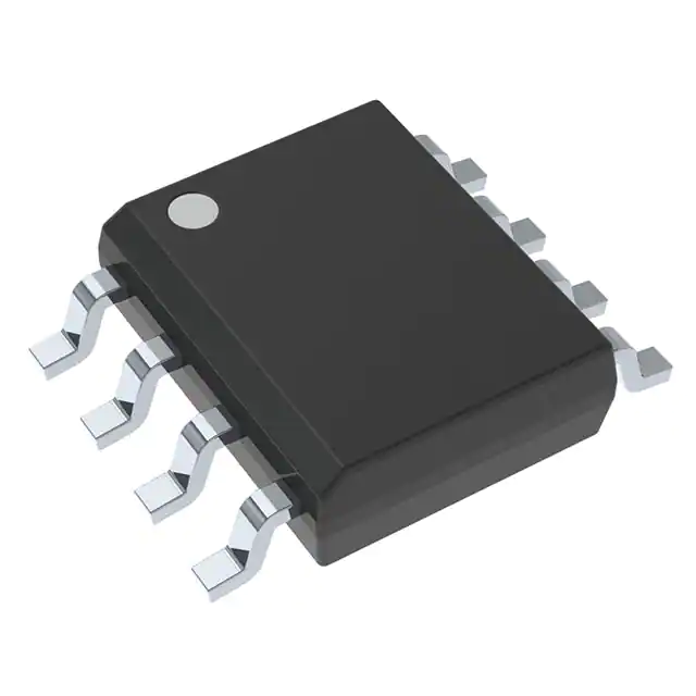
The SN65HVD178x devices are designed to survive overvoltage faults such as direct shortsto power supplies, mis-wiring faults, connector failures, cable crushes, and tool mis-applications.The devices are also robust to ESD events with high levels of protection to the human-body-modelspecification.
The SN65HVD178x devices combine a differential driver and a differential receiver, whichoperate from a single power supply. In the SN65HVD1782, the driver differential outputs and thereceiver differential inputs are connected internally to form a bus port suitable for half-duplex(two-wire bus) communication. This port features a wide common-mode voltage range, making thedevices suitable for multipoint applications over long cable runs. These devices are characterizedfrom –40°C to 125°C. These devices are pin-compatible with the industry-standard SN75176transceiver,making them drop-in upgrades in most systems.
These devices are fully compliant with ANSI TIA/EIA 485-A with a 5-V supply and canoperate with a 3.3-V supply with reduced driver output voltage for low-power applications. Forapplications where operation is required over an extended common-mode voltage range, see theSN65HVD1785 (SLLS872) data sheet.
Feature
- Bus-Pin Fault Protection to:
- > ±70 V (SN65HVD1780,SN65HVD1781)
- > ±30 V (SN65HVD1782)
- Operation With 3.3-V to 5-V Supply Range
- ±16-kV HBM Protectionon Bus Pins
- Reduced Unit Load for Up to 320 Nodes
- FailsafeReceiver for Open-Circuit, Short-Circuit, and Idle-Bus Conditions
- Low Power Consumption
- Low Standby Supply Current,1 μA Maximum
- ICC 4-mA Quiescent Current DuringOperation
- Pin-Compatible With Industry-StandardSN75176
- Signaling Rates of 115 kbps, 1 Mbps, and up to 10Mbps
- Create a Custom Design using the SN65HVD178x with theWEBENCH?Power Designer
All trademarks are the property of their respective owners.


