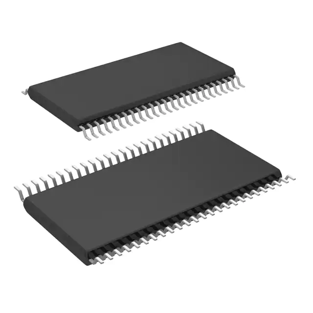
The DS90CF364AMTD/NOPB is a LVDS Receiver converts the four LVDS data streams (up to 1.8Gbps throughput or 227Mbps bandwidth) back into parallel 28 bits of CMOS/TTL data (24 bits of RGB and 4 bits of Hsync, Vsync, DE and CNTL). Also available is the DS90CF364A that converts the three LVDS data streams (up to 1.3Gbps throughput or 170Mbps bandwidth) back into parallel 21 bits of CMOS/TTL data (18 bits of RGB and 3 bits of Hsync, Vsync and DE). Both receiver outputs are falling edge strobe. A rising edge or falling edge strobe transmitter (DS90C383A/DS90C363A) will interoperate with a falling edge strobe receiver without any translation logic. The device is enhanced over prior generation receiver and provided a wider data valid time on the receiver output. This chipset is an ideal means to solve EMI and cable size problems associated with wide, high speed TTL interfaces.
Feature
- 50% Duty cycle on receiver output clock
- Best-in-class set and hold times on RxOUTPUTs
- Rx power consumption of <142mW (typical) at 65MHz grayscale
- Rx power-down mode of <200µW (maximum)
- ESD rating of >7kV (HBM) and >700V (EIAJ)
- Supports VGA, SVGA, XGA and dual pixel SXGA
- PLL requires no external components
- 20 to 65MHz Shift clock support
- Green product and no Sb/Br


