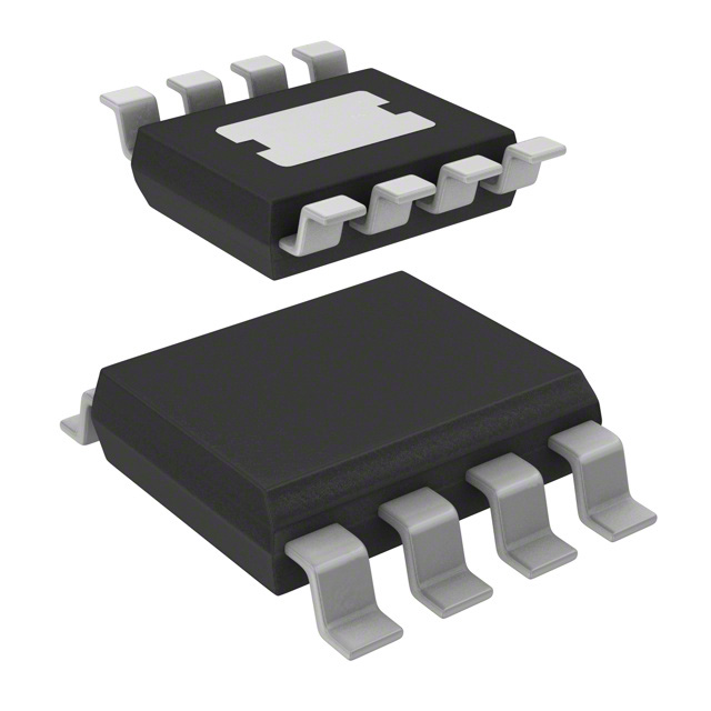
The LTC6090/LTC6090-5 are high voltage, precision monolithic operational amplifiers. The LTC6090HS8E is unity gain stable. The LTC6090-5 is stable in noise gain configurations of 5 or greater. Both amplifiers feature high open loop gain, low input referred offset voltage and noise, and pA input bias current and are ideal for high voltage, high impedance buffering and/or high gain configurations.
The amplifiers are internally protected against overtemperature conditions. A thermal warning output, TFLAG, goes active when the die temperature approaches 150°C. The output stage may be turned off with the output disable pin OD. By tying the OD pin to the thermal warning output (TFLAG), the part will disable the output stage when it is out of the safe operating area. These pins easily interface to any logic family.
Both amplifiers may be run from a single 140V or spit ±70V power supplies and are capable of driving up to 200pF of load capacitance. They are available in either an 8-lead SO or 16-lead TSSOP package with exposed pad for low thermal resistance.
Feature
- Supply Range: ±4.75V to ±70V (140V)
- 0.1Hz to 10Hz Noise: 3.5μVP-P
- Input Bias Current: 50pA Maximum
- Low Offset Voltage: 1.25mV Maximum
- Low Offset Drift: ±5μV/°C Maximum
- CMRR: 130dB Minimum
- Rail-to-Rail Output Stage
- Output Sink and Source: 50mA
- 12MHz Gain Bandwidth Product
- 21V/μs Slew Rate
- 11nV/√Hz Noise Density
- Thermal Shutdown
- Available in Thermally Enhanced SOIC-8E or TSSOP-16E Packages
Applications
- ATE
- Piezo Drivers
- Photodiode Amplifier
- High Voltage Regulators
- Optical Networking
(Picture: Pinout)


