The AD5750/AD5750-1/AD5750-2 are single-channel, low cost, precision voltage/current output drivers with hardware- or software-programmable output ranges. The software ranges are configured via an SPI-/MICROWIRE™-compatible serial interface. The AD5750/AD5750-1/AD5750-2 target applications in PLC and industrial process control. The analog input to the AD5750/ AD5750-1/AD5750-2 is provided from a low voltage, single-supply digital-to-analog converter (DAC) and is internally conditioned to provide the desired output current/voltage range. Analog input ranges available are 0 V to 2.5 V (AD5750-1/AD5750-2) or 0 V to 4.096 V (AD5750).The output current range is programmable across five current ranges: 4 mA to 20 mA, 0 mA to 20 mA or 0 mA to 24 mA, ±20 mA, and ±24 mA. An overrange of 2% is available on the unipolar current ranges.Voltage output is provided from a separate pin that can be configured to provide 0 V to 5 V, 0 V to 10 V, ±5 V, or ±10 V output ranges. An overrange of 20% is available on the voltage ranges.Analog outputs are short-circuit and open-circuit protected and can drive capacitive loads of 1 μF and inductive loads of 0.1 H.The device is specified to operate with a power supply range from ±12 V to ±24 V. Output loop compliance is 0 V to AVDD − 2.75 V.The flexible serial interface is SPI and MICROWIRE compatible and can be operated in 3-wire mode to minimize the digital isolation required in isolated applications. The interface also features an optional PEC error checking feature using CRC-8 error checking, useful in industrial environments where data communication corruption can occur.The device also includes a power-on reset function, ensuring that the device powers up in a known state (0 V or tristate), and an asynchronous CLEAR pin that sets the outputs to zero scale/midscale voltage output or the low end of the selected current range.An HW SELECT pin is used to configure the part for hardware or software mode on power-up.
Feature
- Current output ranges:4 mA to 20 mA, 0 mA to 20 mA or 0 mA to 24 mA, ±20 mA, and ±24 mA ±0.03% FSR total unadjusted error (TUE) ±5 ppm/°C typical output drift
- Voltage output ranges: 0 V to 5 V, 0 V to 10 V, ±5 V, and ±10 V, with 20% overrange ±0.02% FSR TUE ±3 ppm/°C typical output drift
- Flexible serial digital interface
- On-chip output fault detection
- PEC error checking
- Asynchronous CLEAR function
- Flexible power-up condition to 0 V or tristate
- Power supply rangeAVDD: +12 V (± 10%) to +24 V (± 10%)AVSS: −12 V (± 10%) to −24 V (± 10%)
- Output loop compliance to AVDD − 2.75 V
- Temperature range: −40°C to +105°C
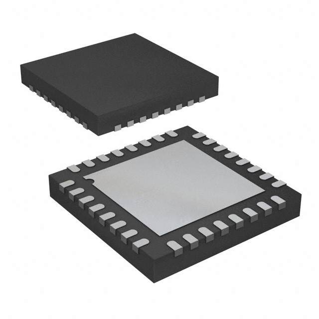
- 32-lead 5 mm × 5 mm LFCSP package
Applications
- Process Control
- Actuator Control
- PLCs
(Picture: Pinout)


