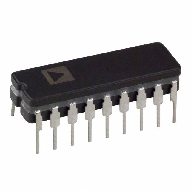
The AMP011 is a monolithic instrumentation amplifierdesigned for high-precision data acquisition and instrumentationapplications. The design combines the conventionalfeatures of an instrumentation amplifier with a high currentoutput stage. The output remains stable with high capacitanceloads (1 μF), a unique ability for an instrumentation amplifier.Consequently, the AMP01BX can amplify low level signals fortransmission through long cables without requiring an outputbuffer. The output stage can be configured as a voltage orcurrent generator.
Input offset voltage is very low (20 μV), which generallyeliminates the external null potentiometer. Temperature changeshave minimal effect on offset; TCVIOS is typically 0.15 μV/°C.Excellent low frequency noise performance is achieved with aminimal compromise on input protection. The bias current isvery low, less than 10 nA over the military temperature range.High common-mode rejection of 130 dB, 16-bit linearity at again of 1000, and 50 mA peak output current are achievablesimultaneously. This combination takes the instrumentationamplifier one step further towards the ideal amplifier.
AC performance complements the superb dc specifications. TheAMP01BX slews at 4.5 V/μs into capacitive loads of up to 15 nF, settlesin 50 μs to 0.01% at a gain of 1000, and boasts a healthy 26 MHzgain bandwidth product. These features make the AMP01BX idealfor high speed data acquisition systems.
The gain is set by the ratio of two external resistors over a range of0.1 to 10,000. A very low gain temperature coefficient of 10 ppm/°Cis achievable over the whole gain range. Output voltage swing isguaranteed with three load resistances: 50 Ω, 500 Ω, and 2 kΩ.Loaded with 500 Ω, the output delivers ±13.0 V minimum. Athermal shutdown circuit prevents destruction of the outputtransistors during overload conditions.
The AMP01BX can also be configured as a high performanceoperational amplifier. In many applications, the AMP01BX can beused in place of op amp/power buffer combinations.
1 Protected under U.S. Patents 4,471,321 and 4,503,381.
Feature
- Low offset voltage: 50 μV maximum
- Very low offset voltage drift: 0.3 μV/°C maximum
- Low noise: 0.12 μV p-p (0.1 Hz to 10 Hz)
- Excellent output drive: ±10 V at ±50 mA
- Capacitive load stability: up to 1 μF
- Gain range: 0.1 to 10,000
- Excellent linearity: 16-bit at G = 1000
- High CMR: 125 dB minimum (G = 1000)
- Low bias current: 4 nA maximum
- Can be configured as a precision op amp
- Output-stage thermal shutdown
- Available in die form
(Picture: Pinout)


