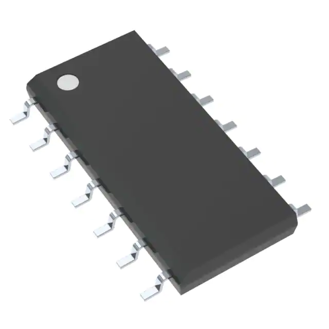
These bus buffer gates feature independent line drivers with 3-state outputs. Each output is disabled when the associated output-enable (OE)\ input is high.
To ensure the high-impedance state during power up or power down, OE\ should be tied to VCC through a pullup resistor; the minimum value of the resistor is determined by the current-sinking capability of the driver.
Feature
- Operating Voltage Range of 4.5 V to 5.5 V
- High-Current Outputs Drive Up To 15 LSTTL Loads
- Low Power Consumption, 80-μA Max ICC
- Typical tpd = 12 ns
- ±6-mA Output Drive at 5 V
- Low Input Current of 1 μA Max
- Inputs Are TTL-Voltage Compatible
- High-Current 3-State Outputs Drive Bus Lines or Buffer Memory Address Registers
These bus buffer gates feature independent line drivers with 3-state outputs. Each output is disabled when the associated output-enable (OE)\ input is high.
To ensure the high-impedance state during power up or power down, OE\ should be tied to VCC through a pullup resistor; the minimum value of the resistor is determined by the current-sinking capability of the driver.


