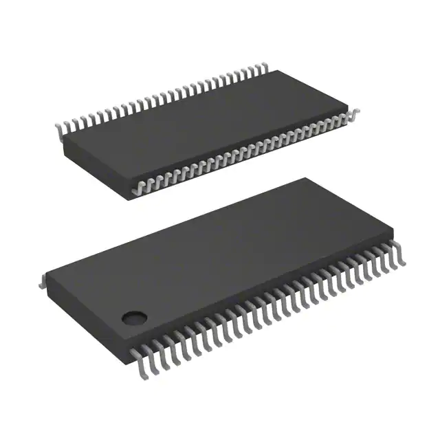
The LCX16543 contains sixteen non-inverting transceivers containing two sets of D-type registers for temporary storage of data flowing in either direction. Each byte has separate control inputs which can be shorted together for full 16-bit operation. Separate Latch Enable and Output Enable inputs are provided for each register to permit independent input and output control in either direction of data flow. The LCX16543 is designed for low voltage (2.5V or 3.3V) VCC applications with capability of interfacing to a 5V signal environment. The LCX16543 is fabricated with an advanced CMOS technology to achieve high speed operation while maintaining CMOS low power dissipation.
Feature
- 5V tolerant inputs and outputs
- 2.3V-3.6V VCC specifications provided
- 5.2 ns tPD max (VCC = 3.3V), 20 µA ICC max
- Power down high impedance inputs and outputs
- Supports live insertion/withdrawal (Note 1)
- ±24 mA Output Drive (VCC = 3.0V)
- Implements patented noise/EMI reduction circuitry
- Latch-up performance exceeds 500 mA
- ESD performance: Human Body Model > 2000V Machine Model > 200V
Applications
- This product is general usage and suitable for many different applications.


