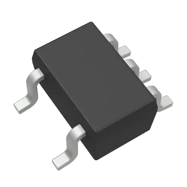
SN74LV1T125DCKR is a low voltage CMOS gate logic that operates at a wider voltage range for industrial, portable, telecom, and automotive applications. The output level is referenced to the supply voltage and is able to support 1.8V/2.5V/3.3V/5V CMOS levels.
The input is designed with a lower threshold circuit to match 1.8V input logic at VCC = 3.3V and can be used in 1.8V to 3.3V level up translation. In addition, the 5V tolerant input pins enable down translation (e.g. 3.3V to 2.5V output at VCC = 2.5V). The wide VCC range of 1.8V to 5.5V allows generation of desired output levels to connect to controllers or processors.
The SN74LV1T125DCKR is designed with current-drive capability of 8 mA to reduce line reflections, overshoot, and undershoot caused by high-drive outputs.
Feature
- Single-Supply Voltage Translator at 5.0/3.3/2.5/1.8V VCC
- Operating Range of 1.8V to 5.5V
- Up Translation
- 1.2V(1) to 1.8V at 1.8V VCC
- 1.5V(1) to 2.5V at 2.5V VCC
- 1.8V(1) to 3.3V at 3.3V VCC
- 3.3V to 5.0V at 5.0VVCC
- Down Translation
- 3.3V to 1.8V at 1.8V VCC
- 3.3V to 2.5V at 2.5V VCC
- 5.0V to 3.3V at 3.3V VCC
- Logic Output is Referenced to VCC
- Output Drive
- 8.0mA Output Drive at 5.0V
- 7.0mA Output Drive at 3.3V
- 3.0mA Output Drive at 1.8V
- Characterized up to 50MHz at 3.3V VCC
- 5.0V Tolerance on Input Pins
- –40°C to 125°C Operating Temperature Range
- Latch-Up Performance Exceeds 250mA
Per JESD 17 - ESD Performance Tested Per JESD 22
- 2000-V Human-Body Model
(A114-B, Class II) - 200-V Machine Model (A115-A)
- 1000-V Charged-Device Model (C101)
- 2000-V Human-Body Model
- Supports Standard Logic Pinouts
- CMOS Output B Compatible with AUP1G and LVC1G Families Refer to the VIH/VIL and output drive for lower VCC condition


