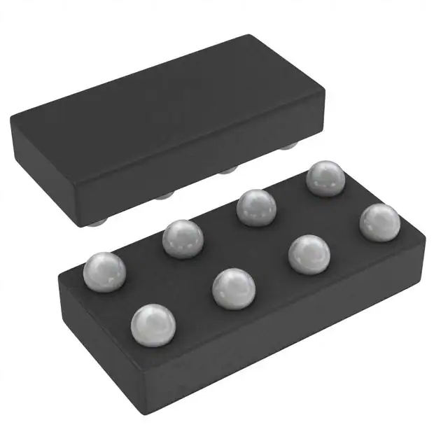
NanoStar is a trademark of Texas Instruments
Texas InstrumentsSN74AUP2G125YZPRThe AUP family is TI’s premier solution to the industry’s low-power needs in battery-powered portable applications. This family ensures a very low static and dynamic power consumption across the entire VCC range of 0.8 V to 3.6 V, resulting in an increased battery life. This product also maintains excellent signal integrity (see Figure 1 and Figure 2).
The SN74AUP2G125YZPR is a dual bus buffer gate designed for 0.8-V to 3.6-V VCC operation. This device features dual line drivers with 3-state outputs. Each output is disabled when the corresponding output-enable (OE should be tied to VCC through a pullup resistor; the minimum value of the resistor is determined by the current-sinking capability of the driver.
NanoStar? package technology is a major breakthrough in IC packaging concepts, using the die as the package.
This device is fully specified for partial-power-down applications using Ioff. The Ioff circuitry disables the outputs, preventing damaging current backflow through the device when it is powered down.
Feature
- Available in the Texas Instruments NanoStar Package
- Low Static-Power Consumption
(ICC = 0.9 μA Max) - Low Dynamic-Power Consumption
(Cpd = 4 pF Typ at 3.3 V) - Low Input Capacitance (CI = 1.5 pF Typ)
- Low Noise – Overshoot and Undershoot
<10% of VCC - Input-Disable Feature Allows Floating Input Conditions
- Ioff Supports Partial-Power-Down Mode Operation
- Input Hysteresis Allows Slow Input Transition and Better Switching
Noise Immunity at Input - Wide Operating VCC Range of 0.8 V to 3.6 V
- Optimized for 3.3-V Operation
- 3.6-V I/O Tolerant to Support Mixed-Mode Signal Operation
- tpd = 5.4 ns Max at 3.3 V
- Suitable for Point-to-Point Applications
- Latch-Up Performance Exceeds 100 mA Per JESD 78, Class II
- ESD Performance Tested Per JESD 22
- 2000-V Human-Body Model
(A114-B, Class II) - 1000-V Charged-Device Model (C101)
- 2000-V Human-Body Model


