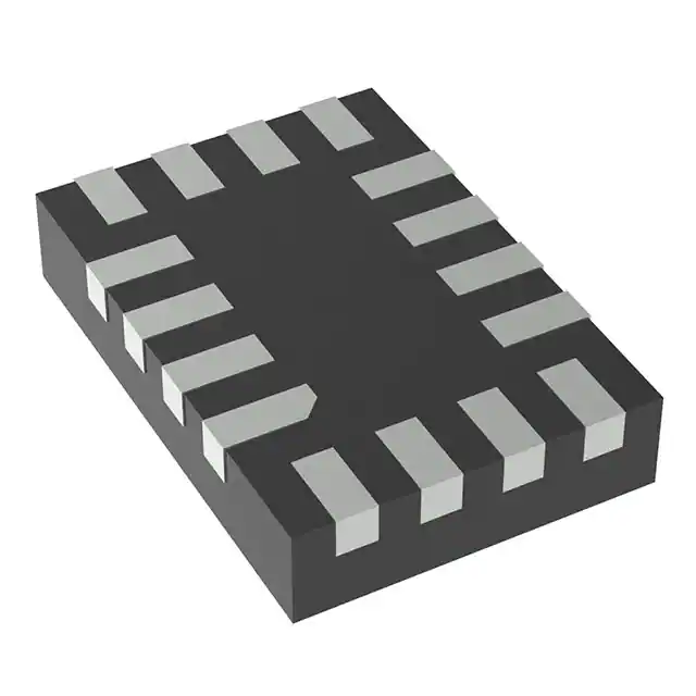
The SN74AXCH4T245RSVR is a four-bit noninverting bus transceiver that uses two individuallyconfigurable power-supply rails. The device is operational with both VCCAand VCCB supplies as low as 0.65 V. The A port is designed to trackVCCA, which accepts any supply voltage from 0.65 V to 3.6 V. The B port isdesigned to track VCCB, which accepts any supply voltage from 0.65 V to 3.6V. The SN74AXCH4T245RSVR device is compatible with a single-supply system.
The SN74AXCH4T245RSVR device is designed for asynchronous communication between data busesand transmits data from the A bus to the B bus or from the B bus to the A bus, depending on thelogic level of the direction-control inputs (1DIR and 2DIR). The output-enable inputs(1OE and 2OE) are used to disable the outputs so thebuses are effectively isolated. All control pins (xDIR and xOE) arereferenced to VCCA.
Active bus-hold circuitry holds unused or undriven inputs at a valid logic state. Use ofpullup or pulldown resistors with the bus-hold circuitry is not recommended. If a supply is presentfor VCCA or VCCB, the bus-hold circuitry alwaysremains active on the A or B inputs respectively, independent of the state of the direction controlor output enable pins.
To ensure the high-impedance state of the level shifter I/Os during power up or powerdown, the xOE pins should be tied to VCCA through apullup resistor.
This device is fully specified for partial-power-down applications using theIoff current. The Ioff protection circuitry ensuresthat no excessive current is drawn from or sourced into an input, output, or combined I/O that isbiased to a specific voltage while the device is powered down.
The VCC isolation feature ensures that if eitherVCCA or VCCB is less than 100 mV, all I/O ports entera high-impedance state by disabling the outputs.
Glitch-free power supply sequencing allows either supply rail to be powered on or off inany order while providing robust power sequencing performance.
Feature
- Fully configurable dual-rail design allows each port to operate with a power supply range from 0.65 V to 3.6 V
- Bus-hold on data inputs eliminates the need for external pullup or pulldown resistors
- Operating temperature from –40°C to +125°C
- Multiple direction control pins to allow simultaneous up and down translation
- Glitch-free power supply sequencing
- Up to 380 Mbps support when translating from 1.8 V to 3.3 V
- VCC isolation feature
- Ioff supports partial-power-down mode operation
- Compatible with AVC family level shifters
- Latch-up performance exceeds 100 mA per JESD 78, Class II
- ESD protection exceeds JESD 22
- 8000-V Human-body model
- 1000-V Charged-device model


