
The AUP family of devices is TI’s premier solution to the industry’s low-power needs inbattery-powered portable applications. This family ensures a very low static- and dynamic-powerconsumption across the entire VCC range of 0.8 V to 3.6 V, resulting inincreased battery life. This product also maintains excellent signal integrity (seeAUP – The Lowest-Power Family and Excellent Signal Integrity).
This device functions as an independent gate with Schmitt-trigger inputs, which allowsfor slow input transition and better switching-noise immunity at the input.
NanoStar package technology is a major breakthrough in IC packaging concepts, using thedie as the package.
This device is fully specified for partial-power-down applications usingIoff. The Ioff circuitry disables the outputs whenthe device is powered down. This inhibits current backflow into the device which prevents damage tothe device.
Feature
- Latch-Up Performance Exceeds 100 mA Per JESD 78, Class II
- ESD Performance Tested Per JESD 22
- 2000-V Human-Body Model
(A114-B, Class II) - 1000-V Charged-Device Model (C101)
- 2000-V Human-Body Model
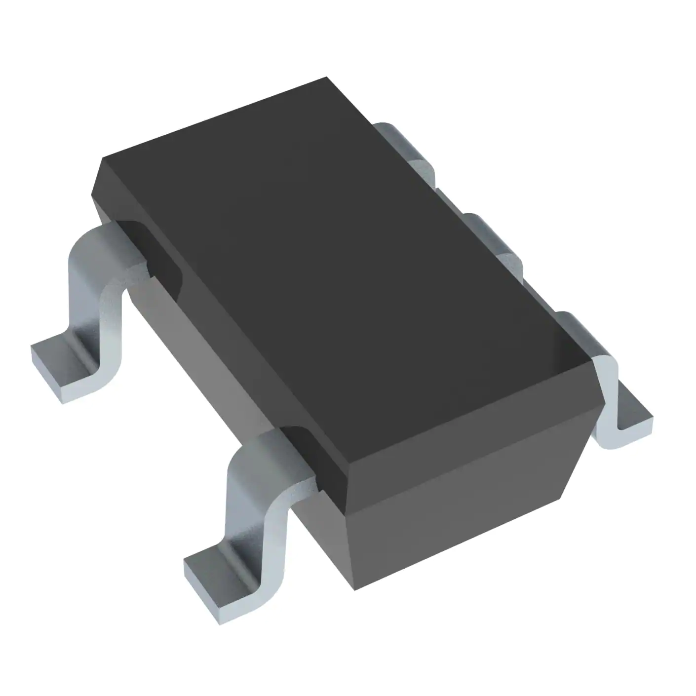
- Available in the Texas Instruments NanoStar Package
- Low Static-Power Consumption
(ICC = 0.9 μA Maximum) - Low Dynamic-Power Consumption
(Cpd = 4.4 pF Typical at 3.3 V) - Low Input Capacitance (Ci = 1.5 pF Typical)
- Low Noise – Overshoot and Undershoot
<10% of VCC - Ioff Supports Partial-Power-Down Mode Operation
- Includes Schmitt-Trigger Inputs
- Wide Operating VCC Range of 0.8 V to 3.6 V
- Optimized for 3.3-V Operation
- 3.6-V I/O Tolerant to Support Mixed-Mode Signal Operation
- tpd = 5.1 ns Maximum at 3.3 V
- Suitable for Point-to-Point Applications


