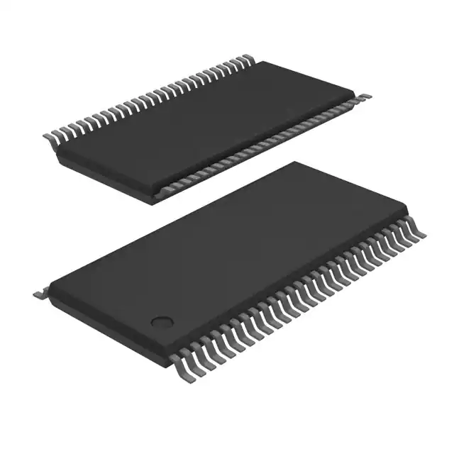
Widebus is a trademark of Texas Instruments.
DescriptionThe 'ABT16825 devices are 18-bit buffers and line drivers designed specifically to improve both the performance and density of 3-state memory address drivers, clock drivers, and bus-oriented receivers and transmitters. These devices can be used as two 9-bit buffers or one 18-bit buffer. They provide true data.
The 3-state control gate is a 2-input AND gate with active-low inputs so that, if either output-enable (OE1\ or OE2\) input is high, all nine affected outputs are in the high-impedance state.
When VCC is between 0 and 2.1 V, the device is in the high-impedance state during power up or power down. However, to ensure the high-impedance state above 2.1 V, OE\ should be tied to VCC through a pullup resistor; the minimum value of the resistor is determined by the current-sinking capability of the driver.
Feature
- Members of Texas Instruments' WidebusTM Family
- Latch-Up Performance Exceeds 500 mA Per JEDEC Standard JESD 17
- Typical VOLP (Output Ground Bounce) <1 V at VCC = 5 V, TA = 25°C
- High-Impedance State During Power Up and Power Down
- Distributed VCC and GND PinsMinimize High-Speed Switching Noise
- Flow-Through Architecture Optimizes PCB Layout
- High-Drive Outputs (-32-mA IOH, 64-mA IOL)
Widebus is a trademark of Texas Instruments.
DescriptionThe 'ABT16825 devices are 18-bit buffers and line drivers designed specifically to improve both the performance and density of 3-state memory address drivers, clock drivers, and bus-oriented receivers and transmitters. These devices can be used as two 9-bit buffers or one 18-bit buffer. They provide true data.
The 3-state control gate is a 2-input AND gate with active-low inputs so that, if either output-enable (OE1\ or OE2\) input is high, all nine affected outputs are in the high-impedance state.
When VCC is between 0 and 2.1 V, the device is in the high-impedance state during power up or power down. However, to ensure the high-impedance state above 2.1 V, OE\ should be tied to VCC through a pullup resistor; the minimum value of the resistor is determined by the current-sinking capability of the driver.


