久芯网

74LVC1G125GW/DG,12

  • 描述:逻辑类型: 缓冲区,非反相 电源电压: 1.65伏~5.5伏 每个元件的位数: one 供应商设备包装: 5-TSSOP 工作温度: -40摄氏度~125摄氏度(TA) 安装类别: 表面安装
  • 品牌: 恩智浦 (NXP)
  • 交期:5-7 工作日
渠道:
  • 自营
  • 得捷
  • 贸泽

起订量: 1

  • 库存: 0
  • 单价: ¥3.82425
  • 数量:
    - +
  • 总计: ¥3.82
在线询价

温馨提示: 请填写以下信息,以便客户代表及时与您沟通联系。

规格参数

  • 逻辑类型 缓冲区,非反相
  • 元件数量 one
  • 输入类别 -
  • 输出类别 三态
  • 工作温度 -40摄氏度~125摄氏度(TA)
  • 安装类别 表面安装
  • 部件状态 过时的
  • 制造厂商 恩智浦 (NXP)
  • 每个元件的位数 one
  • 电源电压 1.65伏~5.5伏
  • 输出高电流, 输出低电流 32毫安, 32毫安
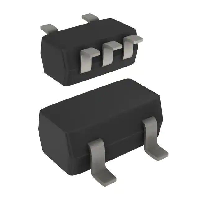
  • 包装/外壳 5-TSSOP, SC-70-5, SOT-353
  • 供应商设备包装 5-TSSOP

74LVC1G125GW/DG,12 产品详情

The 74LVC1G125GW,125 is a non-inverting buffer/Line Driver with 3-state output. The 3-state output is controlled by the output enable input (OE). A high-level at pin OE causes the output to assume a high-impedance off-state. The input can be driven from either 3.3 or 5V devices. This feature allows the use of this device in a mixed 3.3 and 5V environment. This device is fully specified for partial power-down applications using IOFF. The IOFF circuitry disables the output, preventing the damaging backflow current through the device when it is powered down.

Feature

  • High noise immunity
  • ±24mA Output drive (VCC=3.0V)
  • CMOS Low power consumption
  • Inputs accept voltages up to 5V
  • Latch-up performance exceeds 250mA
  • Direct interface with TTL levels
  • Complies with JEDEC standard
74LVC1G125GW/DG,12所属分类:逻辑接收/发送/驱动/缓冲器,74LVC1G125GW/DG,12 由 恩智浦 (NXP) 设计生产,可通过久芯网进行购买。74LVC1G125GW/DG,12价格参考¥3.824251,你可以下载 74LVC1G125GW/DG,12中文资料、PDF数据手册、Datasheet数据手册功能说明书,可查询74LVC1G125GW/DG,12规格参数、现货库存、封装信息等信息!

恩智浦 (NXP)

恩智浦 (NXP)

NXP Semiconductors是一家领先的嵌入式控制器供应商,为汽车、无线连接等多个行业提供广泛的MCU产品组合,包括基于Arm的处理器和微控制器。他们继续推动创新,为工业和汽车应用提供强大的电源...

展开
会员中心 微信客服
客服
回到顶部