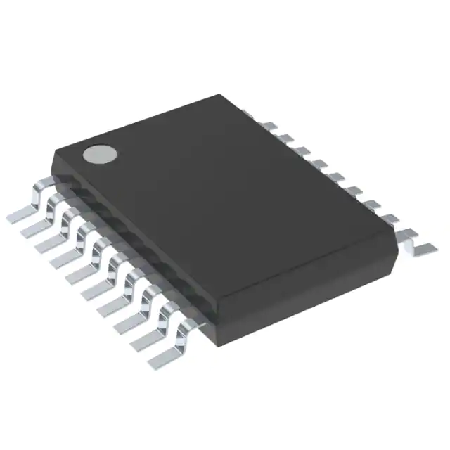
The SN54BCT540 and SN74BCT540ANSR octal buffers and line drivers are ideal for driving bus lines or buffer memory-address registers. The devices feature inputs and outputs on opposite sides of the package to facilitate printed circuit board layout.
The 3-state control gate is a 2-input AND gate with active-low inputs so that if either output-enable (OE1\ or OE2\) input is high, all corresponding outputs are in the high-impedance state.
To ensure the high-impedance state during power up or power down, OE\ should be tied to VCC through a pullup resistor; the minimum value of the resistor is determined by the current-sinking capability of the driver.
Feature
- Operating Voltage Range of 4.5 V to 5.5 V
- State-of-the-Art BiCMOS Design Significantly Reduces ICCZ
- 3-State Outputs Drive Bus Lines or Buffer Memory Address Registers
- P-N-P Inputs Reduce DC Loading
- Data Flow-Through Pinout (All Inputs on Opposite Side From Outputs)
- ESD Protection Exceeds JESD 22
- 2000-V Human-Body Model (A114-A)
- 200-V Machine Model (A115-A)
- 1000-V Charged-Device Model (C101)


