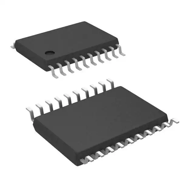
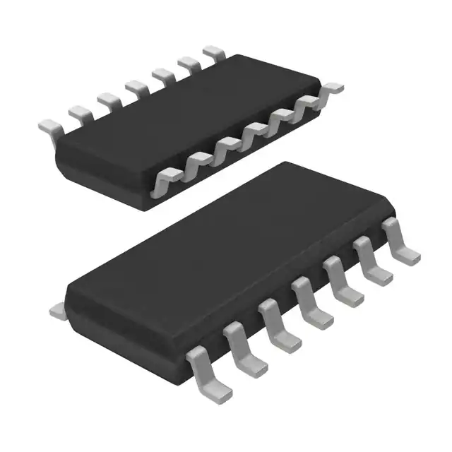
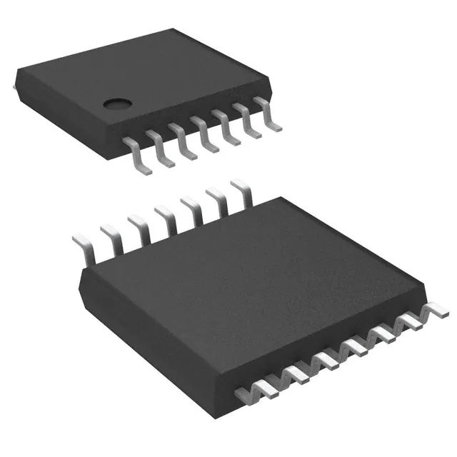
The VHC112 is an advanced high speed CMOS device fabricated with silicon gate CMOS technology. It achieves the high-speed operation similar to equivalent Bipolar Schottky TTL while maintaining the CMOS low power dissipation. The VHC112 contains two independent, high-speed JK flip-flops with Direct Set and Clear inputs. Synchronous state changes are initiated by the falling edge of the clock. Triggering occurs at a voltage level of the clock and is not directly related to transition time. The J and K inputs can change when the clock is in either state without affecting the flip-flop, provided that they are in the desired state during the recommended setup and hold times relative to the falling edge of the clock. The LOW signal on PR or CLR prevents clocking and forces Q and Q# HIGH, respectively. Simultaneous LOW signals on PR and CLR force both Q and Q# HIGH. An input protection circuit ensures that 0V to 7V can be applied to the input pins without regard to the supply voltage. This device can be used to interface 5V to 3V systems and two supply systems such as battery backup. This circuit prevents device destruction due to mismatched supply and input voltages.
Feature
- High speed: fMAX = 200 MHz (typ) at VCC = 5.0V
- Low power dissipation: ICC = 2 µA (max) at TA = 25°C
- High noise immunity: VNIH = VNIL = 28% VCC (min)
- Power down protection is provided on all inputs
- Pin and function compatible with 74HC112
Applications
- This product is general usage and suitable for many different applications.


