All trademarks are the property of their respective owners.
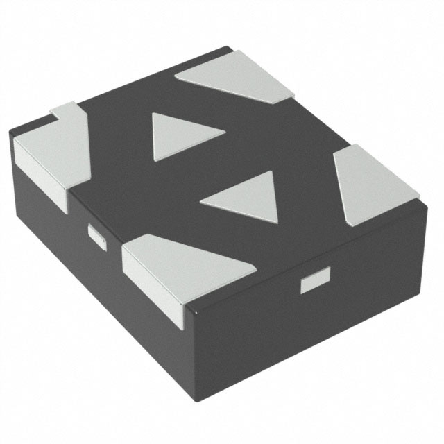
DescriptionThe SN74AXCH1T45DTQR is a single-bit noninverting bus transceiver that uses two individuallyconfigurable power-supply rails. The device is operational with both VCCAand VCCB supplies as low as 0.65 V. The A port is designed to trackVCCA, which accepts any supply voltage from 0.65 V to 3.6 V. The B port isdesigned to track VCCB, which also accepts any supply voltage from 0.65 V to3.6 V. Additionally the SN74AXCH1T45DTQR is compatible with a single-supply system.
The DIR pin determines the direction of signal propagation. With the DIR pin configuredHIGH, translation is from Port A to Port B. With DIR configured LOW, translation is from Port B toPort A. The DIR pin is referenced to VCCA, meaning that its logic-high andlogic-low thresholds track with VCCA.
Active bus-hold circuitry holds unused or undriven inputs at a valid logic state. Use ofpullup or pulldown resistors with the bus-hold circuitry is not recommended. If a supply is presentfor VCCA or VCCB, the bus-hold circuitry alwaysremains active on the A or B inputs respectively, independent of the state of the direction controlpin.
This device is fully specified for partial-power-down applications using theIoff current. The Ioff protection circuitry ensuresthat no excessive current is drawn from or to an input, output, or combined I/O that is biased to aspecific voltage while the device is powered down.
The VCC isolation feature ensures that if eitherVCCA or VCCB is less than 100 mV, both I/O portsenter a high-impedance state by disabling their outputs.
Glitch-free power supply sequencing allows either supply rail to be powered on or off inany order while providing robust power sequencing performance.
Feature
- Fully Configurable Dual-Rail Design Allows Each Port to Operate With a Power SupplyRange from 0.65 V to 3.6 V
- Operating Temperature: –40°C to +125°C
- Glitch-Free Power Supply Sequencing
- Bus-hold on Data InputsEliminates the Need for External Pullup or Pulldown Resistors
- Maximum QuiescentCurrent (ICCA + ICCB) of 8 μA (85°C Maximum) and 14μA (125°C Maximum)
- Up to 500-Mbps Support When Translating from 1.8 to3.3V
- VCC Isolation Feature
- If Either VCC Input is Below 100 mV, All I/Os Outputsare Disabled and Become High-Impedance
- Ioff Supports Partial-Power-Down Mode Operation
- Latch-Up Performance Exceeds 100 mA Per JESD 78, Class II
- ESD Protection Exceeds JESD 22
- 8000-V Human Body Model
- 1000-V Charged-DeviceModel
All trademarks are the property of their respective owners.
DescriptionThe SN74AXCH1T45 is a single-bit noninverting bus transceiver that uses two individuallyconfigurable power-supply rails. The device is operational with both VCCAand VCCB supplies as low as 0.65 V. The A port is designed to trackVCCA, which accepts any supply voltage from 0.65 V to 3.6 V. The B port isdesigned to track VCCB, which also accepts any supply voltage from 0.65 V to3.6 V. Additionally the SN74AXCH1T45 is compatible with a single-supply system.
The DIR pin determines the direction of signal propagation. With the DIR pin configuredHIGH, translation is from Port A to Port B. With DIR configured LOW, translation is from Port B toPort A. The DIR pin is referenced to VCCA, meaning that its logic-high andlogic-low thresholds track with VCCA.
Active bus-hold circuitry holds unused or undriven inputs at a valid logic state. Use ofpullup or pulldown resistors with the bus-hold circuitry is not recommended. If a supply is presentfor VCCA or VCCB, the bus-hold circuitry alwaysremains active on the A or B inputs respectively, independent of the state of the direction controlpin.
This device is fully specified for partial-power-down applications using theIoff current. The Ioff protection circuitry ensuresthat no excessive current is drawn from or to an input, output, or combined I/O that is biased to aspecific voltage while the device is powered down.
The VCC isolation feature ensures that if eitherVCCA or VCCB is less than 100 mV, both I/O portsenter a high-impedance state by disabling their outputs.
Glitch-free power supply sequencing allows either supply rail to be powered on or off inany order while providing robust power sequencing performance.


