Features
■ Enhanced configuration devices include EPC4, EPC8, and EPC16 devices
■ Single-chip configuration solution for Stratix® series, Cyclone™ series, APEX™ II, APEX 20K (including APEX 20K, APEX 20KC, and APEX 20KE), Mercury™, ACEX® 1K, and FLEX® 10K (FLEX 10KE and FLEX 10KA) devices
■ Contains 4-, 8-, and 16-Mbit flash memories for configuration data storage
● On-chip decompression feature almost doubles the effective configuration density
■ Standard flash die and a controller die combined into single stacked chip package
■ External flash interface supports parallel programming of flash and external processor access to unused portions of memory
● Flash memory block/sector protection capability via external flash interface
● Supported in EPC16 and EPC4 devices
■ Page mode support for remote and local reconfiguration with up to eight configurations for the entire system
● Compatible with Stratix series Remote System Configuration feature
■ Supports byte-wide configuration mode fast passive parallel (FPP); 8-bit data output per DCLK cycle
■ Supports true n-bit concurrent configuration (n = 1, 2, 4, and 8) of Altera FPGAs
■ Pin-selectable 2-ms or 100-ms power-on reset (POR) time
■ Configuration clock supports programmable input source and frequency synthesis
● Multiple configuration clock sources supported (internal oscillator and external clock input pin)
● External clock source with frequencies up to 133 MHz
● Internal oscillator defaults to 10 MHz; Programmable for higher frequencies of 33, 50, and 66 MHz
● Clock synthesis supported via user programmable divide counter
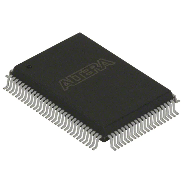
■ Available in the 100-pin plastic quad flat pack (PQFP) and the 88-pin Ultra FineLine BGA® packages
● Vertical migration between all devices supported in the 100-pin PQFP package
■ Supply voltage of 3.3 V (core and I/O)
■ Hardware compliant with IEEE Std. 1532 in-system programmability (ISP) specification
■ Supports ISP via Jam Standard Test and Programming Language (STAPL)
■ Supports Joint Test Action Group (JTAG) boundary scan
■ nINIT_CONF pin allows private JTAG instruction to initiate FPGA configuration
■ Internal pull-up resistor on nINIT_CONF always enabled
■ User programmable weak internal pull-up resistors on nCS and OE pins
■ Internal weak pull-up resistors on external flash interface address and control lines, bus hold on data lines
■ Standby mode with reduced power consumption
Functional Description
The Altera enhanced configuration device is a single-device, high-speed, advanced configuration solution for very high-density FPGAs. The core of an enhanced configuration device is divided into two major blocks, a configuration controller and a flash memory. The flash memory is used to store configuration data for systems made up of one or more Altera FPGAs. Unused portions of the flash memory can be used to store processor code or data that can be accessed via the external flash interface after FPGA configuration is complete.
The enhanced configuration device has a 3.3-V core and I/O interface. The controller chip is a synchronous system that implements the various interfaces and features. Figure 2–1 shows a block diagram of the enhanced configuration device. The controller chip features three separate interfaces:
■ A configuration interface between the controller and the Altera FPGA(s)
■ A JTAG interface on the controller that enables in-system programmability (ISP) of the flash memory
■ An external flash interface that the controller shares with an external processor, or FPGA implementing a Nios® embedded processor (interface available after ISP and configuration)
Feature
High-performance CMOS EEPROM-based programmable logic devices (PLDs) built on third-generation Multiple Array MatriX (MAX®) architecture
■ 5.0-V in-system programmability (ISP) through built-in IEEE Std. 1149.1 Joint Test Action Group (JTAG) interface■ Built-in JTAG boundary-scan test (BST) circuitry compliant with IEEE Std. 1149.1-1990
■ High-density erasable programmable logic device (EPLD) family ranging from 6,000 to 12,000 usable gates (see Table 1)
■ 10-ns pin-to-pin logic delays with counter frequencies of up to 144 MHz
■ Fully compliant with the peripheral component interconnect Special Interest Group’s (PCI SIG) PCI Local Bus Specification, Revision 2.2
■ Dual-output macrocell for independent use of combinatorial and registered logic
■ FastTrack® Interconnect for fast, predictable interconnect delays
■ Input/output registers with clear and clock enable on all I/O pins
■ Programmable output slew-rate control to reduce switching noise
■ MultiVolt™ I/O interface operation, allowing devices to interface with 3.3-V and 5.0-V devices
■ Configurable expander product-term distribution allowing up to 32 product terms per macrocell
■ Programmable power-saving mode for more than 50% power reduction in each macrocell

