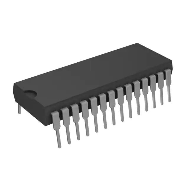
High-performance 64K EEPROM offers access times to 150ns with power dissipation of 220mW. Deselected, CMOS standby current is less than 100µA . It is accessed like static RAM for the read or write cycle without external components. It contains a 64-byte page register to allow writing of up to 64 bytes simultaneously. The EEPROM features Internal error correction for extended endurance and improved data retention. Optional software data protection mechanism guards against inadvertent writes, and an extra 64 bytes of EEPROM enables device identification or tracking.
Feature
The AT28C64B is a high-performance electrically-erasable and programmable readonly memory (EEPROM). Its 64K of memory is organized as 8,192 words by 8 bits. Manufactured with Atmel’s advanced nonvolatile CMOS technology, the device offers access times to 150 ns with power dissipation of just 220 mW. When the device is deselected, the CMOS standby current is less than 100 µA.
The AT28C64B is accessed like a Static RAM for the read or write cycle without the need for external components. The device contains a 64-byte page register to allow writing of up to 64 bytes simultaneously. During a write cycle, the addresses and 1 to 64 bytes of data are internally latched, freeing the address and data bus for other operations. Following the initiation of a write cycle, the device will automatically write the latched data using an internal control timer. The end of a write cycle can be detected by DATA POLLING of I/O7. Once the end of a write cycle has been detected, a new access for a read or write can begin.
Atmel’s AT28C64B has additional features to ensure high quality and manufacturability. The device utilizes internal error correction for extended endurance and improved data retention characteristics. An optional software data protection mechanism is available to guard against inadvertent writes. The device also includes an extra 64 bytes of EEPROM for device identification or tracking.
Features
• Fast Read Access Time – 150 ns
• Automatic Page Write Operation
– Internal Address and Data Latches for 64 Bytes
• Fast Write Cycle Times
– Page Write Cycle Time: 10 ms Maximum (Standard)
2 ms Maximum (Option – Ref. AT28HC64BF Datasheet)
– 1 to 64-byte Page Write Operation
• Low Power Dissipation
– 40 mA Active Current
– 100 µA CMOS Standby Current
• Hardware and Software Data Protection
• DATA Polling and Toggle Bit for End of Write Detection
• High Reliability CMOS Technology
– Endurance: 100,000 Cycles
– Data Retention: 10 Years
• Single 5V ±10% Supply
• CMOS and TTL Compatible Inputs and Outputs
• JEDEC Approved Byte-wide Pinout
• Industrial Temperature Ranges
• Green (Pb/Halide-free) Packaging Option Only
Device Operation
1. Read
The AT28C64B is accessed like a Static RAM. When CE and OE are low and WE is high, the data stored at the memory location determined by the address pins is asserted on the outputs. The outputs are put in the high-impedance state when either CE or OE is high. This dual line control gives designers flexibility in preventing bus contention in their systems.
2 Byte Write
A low pulse on the WE or CE input with CE or WE low (respectively) and OE high initiates a write cycle. The address is latched on the falling edge of CE or WE, whichever occurs last. The data is latched by the first rising edge of CE or WE. Once a byte write has been started, it will automatically time itself to completion. Once a programming operation has been initiated and for the duration of tWC, a read operation will effectively be a polling operation.
3 Page Write
The page write operation of the AT28C64B allows 1 to 64 bytes of data to be written into the device during a single internal programming period. A page write operation is initiated in the same manner as a byte write; after the first byte is written, it can then be followed by 1 to 63 additional bytes. Each successive byte must be loaded within 150 µs (tBLC) of the previous byte. If the tBLC limit is exceeded, the AT28C64B will cease accepting data and commence the internal programming operation. All bytes during a page write operation must reside on the same page as defined by the state of the A6 to A12 inputs. For each WE high to low transition during the page write operation, A6 to A12 must be the same. The A0 to A5 inputs specify which bytes within the page are to be written. The bytes may be loaded in any order and may be altered within the same load period. Only bytes which are specified for writing will be written; unnecessary cycling of other bytes within the page does not occur.


