Feature
- Fast access times - 7.5ns up to 117MHz clock frequency
- LBO input selects interleaved or linear burst mode
- Self-timed write cycle with global write control (GW), byte write enable (BWE), and byte writes (BWx)
- 3.3V core power supply
- Power down controlled by ZZ input
- 3.3V I/O
- Optional - Boundary Scan JTAG Interface (IEEE 1149.1 compliant)
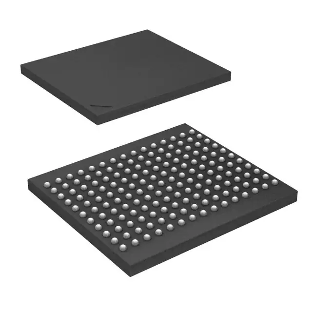
- Available in 100-pin TQFP, 119-pin BGA and 165 fpBGA packages


