All trademarks are the property of their respective owners.
DescriptionThe UCC27212A-Q1 device driver is based on the popularUCC27211 MOSFET drivers. In addition, UCC27212A-Q1 offers extendedoperating range all the way down to 5 V which helps lower power losses.
The peak output pullup and pulldown current is 4-A source and 4-A sink, and pullup andpulldown resistance is 0.9 Ω. This allows for the ability to drive large power MOSFETs withminimized switching losses during the transition through the Miller Plateau of the MOSFET.
The input structure can directly handle –10 V, which increases robustness and also allowsdirect interface to gate-drive transformers without using rectification diodes. The inputs are alsoindependent of supply voltage and have a 20-V maximum rating.
The switching node of the UCC27212A-Q1 (HS pin) can handle–18-V maximum, which allows the high-side channel to be protected from inherent negative voltagescaused by parasitic inductance and stray capacitance. The UCC27212A-Q1 has increased hysteresis that allows for interface to analog ordigital PWM controllers with enhanced noise immunity.
The low-side and high-side gate drivers are independently controlled and matched to 4 nsbetween the turn on and turn off of each other.
An on-chip 100-V rated bootstrap diode eliminates the external discrete diodes.Undervoltage lockout is provided for both the high-side and the low-side drivers which providessymmetric turn on and turn off behavior and forces the outputs low if the drive voltage is belowthe specified threshold.
Feature
- Qualified for AutomotiveApplications
- AECA-Q100 Qualified with thefollowing results:
- Device temperature grade –40°C to +140°C
- Device HBM classification level 2
- Device CDM classification level C6
- 5-V Turn-off Under Voltage Lockout(UVLO)
- Drives Two N-Channel MOSFETs in High-Side andLow-Side Configuration With Independent Inputs
- MaximumBoot Voltage 120-V DC
- 4-A Sink, 4-A Source OutputCurrents
- 0.9-Ω Pullup and Pulldown Resistance
- Input Pins Can Tolerate –10 V to +20 V and are Independentof Supply Voltage Range
- TTL CompatibleInputs
- 5-V to 17-V VDD Operating Range, (20-V ABS Maximum)
- 7.2-ns Rise and 5.5-ns Fall Time With 1000-pF Load
- Fast Propagation Delay Times (20-nstypical)
- 4-ns Typical Delay Matching
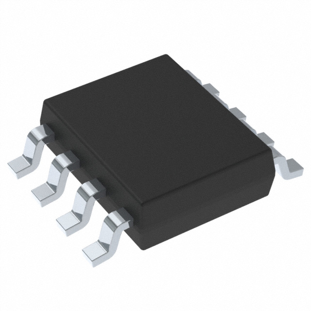
- Available in the SOIC8(Powerpad) package
All trademarks are the property of their respective owners.
DescriptionThe UCC27212A-Q1 device driver is based on the popularUCC27211 MOSFET drivers. In addition, UCC27212A-Q1 offers extendedoperating range all the way down to 5 V which helps lower power losses.
The peak output pullup and pulldown current is 4-A source and 4-A sink, and pullup andpulldown resistance is 0.9 Ω. This allows for the ability to drive large power MOSFETs withminimized switching losses during the transition through the Miller Plateau of the MOSFET.
The input structure can directly handle –10 V, which increases robustness and also allowsdirect interface to gate-drive transformers without using rectification diodes. The inputs are alsoindependent of supply voltage and have a 20-V maximum rating.
The switching node of the UCC27212A-Q1 (HS pin) can handle–18-V maximum, which allows the high-side channel to be protected from inherent negative voltagescaused by parasitic inductance and stray capacitance. The UCC27212A-Q1 has increased hysteresis that allows for interface to analog ordigital PWM controllers with enhanced noise immunity.
The low-side and high-side gate drivers are independently controlled and matched to 4 nsbetween the turn on and turn off of each other.
An on-chip 100-V rated bootstrap diode eliminates the external discrete diodes.Undervoltage lockout is provided for both the high-side and the low-side drivers which providessymmetric turn on and turn off behavior and forces the outputs low if the drive voltage is belowthe specified threshold.


