All trademarks are the property of their respective owners.
DescriptionThe UCC21222-Q1 device is an isolated dual channel gate driver withprogrammable dead time and wide temperature range. This device exhibits consistent performance androbustness under extreme temperature conditions. It is designed with 4-A peak-source and 6-Apeak-sink current to drive power MOSFET, IGBT, and GaN transistors.
The UCC21222-Q1device can be configured as two low-side drivers, two high-side drivers, or a half-bridge driver.5ns delay matching performance allows two outputs to be paralleled, doubling the drive strength forheavy load conditions without risk of internal shoot-through.
The input side is isolated from the two output drivers by a3.0-kVRMS isolation barrier, with a minimum of 100-V/ns common-modetransient immunity (CMTI).
Resistor programmable dead time gives the capability to adjust dead time for systemconstraints to improve efficiency and prevent output overlap. Other protection features include:Disable feature to shut down both outputs simultaneously when DIS is set high, integrated deglitchfilter that rejects input transients shorter than 5-ns, and negative voltage handling for up to-2-V spikes for 200-ns on input and output pins. All supplies have UVLO protection.
Feature
- AEC Q100 Qualified with:
- Device Temperature Grade 1
- Device HBM ESD Classification Level H2
- Device CDM ESD Classification Level C6
- Junction Temperature Range –40°C to150°C
- Resistor-Programmable DeadTime
- Universal: Dual Low-Side, Dual High-Side or Half-Bridge Driver
- 4-A Peak Source, 6-A Peak Sink Output
- 3-V to 5.5-V Input VCCIRange
- Up to 18-V VDD Output Drive Supply
- 8-V VDD UVLO
- Switching Parameters:
- 28-ns Typical Propagation Delay
- 10-ns Minimum PulseWidth
- 5-ns Maximum Delay Matching
- 5.5-ns MaximumPulse-Width Distortion
- TTL and CMOS CompatibleInputs
- Integrated Deglitch Filter
- I/Os withstand –2-V for200 ns
- Common-Mode Transient Immunity (CMTI) Greater than100-V/ns
- Isolation Barrier Life >40 Years
- Surge Immunityup to 7800-VPK
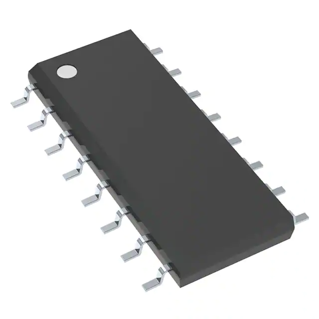
- Narrow Body SOIC-16 (D) Package
- Safety-Related Certifications (Planned):
- 4242-VPK Isolation per DIN V VDE V 0884-11:2017-01 andDIN EN 61010-1
- 3000-VRMS Isolation for 1 Minute per UL1577
- CSA Certification per IEC 60950-1, IEC 62368-1 and IEC 61010-1 EndEquipment Standards
- CQC Certification per GB4943.1-2011
All trademarks are the property of their respective owners.
DescriptionThe UCC21222-Q1 device is an isolated dual channel gate driver withprogrammable dead time and wide temperature range. This device exhibits consistent performance androbustness under extreme temperature conditions. It is designed with 4-A peak-source and 6-Apeak-sink current to drive power MOSFET, IGBT, and GaN transistors.
The UCC21222-Q1device can be configured as two low-side drivers, two high-side drivers, or a half-bridge driver.5ns delay matching performance allows two outputs to be paralleled, doubling the drive strength forheavy load conditions without risk of internal shoot-through.
The input side is isolated from the two output drivers by a3.0-kVRMS isolation barrier, with a minimum of 100-V/ns common-modetransient immunity (CMTI).
Resistor programmable dead time gives the capability to adjust dead time for systemconstraints to improve efficiency and prevent output overlap. Other protection features include:Disable feature to shut down both outputs simultaneously when DIS is set high, integrated deglitchfilter that rejects input transients shorter than 5-ns, and negative voltage handling for up to-2-V spikes for 200-ns on input and output pins. All supplies have UVLO protection.


